SPRUIX0D February 2021 – August 2021
- Trademarks
- 1Introduction
- 2Important Usage Notes
-
3System Description
- 3.1 Key Features
- 3.2 Functional Block Diagram
- 3.3 Power-On/Off Procedures
- 3.4
Peripheral and Major Component
Description
- 3.4.1 Clocking
- 3.4.2 Reset
- 3.4.3 Power
- 3.4.4 Configuration
- 3.4.5 JTAG
- 3.4.6 Test Automation
- 3.4.7 UART Interfaces
- 3.4.8 Memory Interfaces
- 3.4.9 Ethernet Interface
- 3.4.10 Display Interface
- 3.4.11 USB 2.0 Interface
- 3.4.12 PCIe Interface
- 3.4.13 High Speed Expansion Interface
- 3.4.14 CAN Interface
- 3.4.15 Interrupt
- 3.4.16 ADC Interface
- 3.4.17 Safety Connector
- 3.4.18 SPI Interfaces
- 3.4.19 I2C Interfaces
- 3.4.20 FSI Interface
- 4Known Issues and Modifications
- 5References
- 6Revision History
3.4.14 CAN Interface
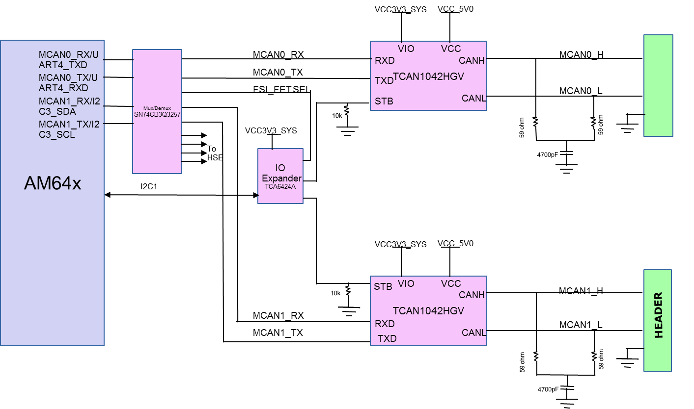
The GP EVM includes two CAN interfaces. The MCAN0 and MCAN1 pins are muxed internally with UART4 and I2C3 respectively. These signals are connected to an on board MUX to route the signals to either the MCAN Transceiver or to the HSE connector, this MUX is controlled by the IO Expander. Figure 3-29 depicts the implementation of CAN interface using TCAN1042HGV. RXD and TXD pins are connected to MCAN0_RX/UART4_TXD and MCAN0_TX/UART4_RXD pins of AM64x respectively. STB pin of the IC is by default connected to ground to avoid IC entering stand-by mode. The STB pin is controlled by GPIO to enable Standby mode.
The pin-out of CAN connector is shown in Table 3-25.
| CAN0 J31 | CAN1 J32 | ||
|---|---|---|---|
| Pin No. | Signal | Pin No. | Signal |
| 1 | MCAN0_H | 1 | MCAN0_H |
| 2 | GND | 2 | GND |
| 3 | MCAN0_L | 3 | MCAN0_L |
 Figure 3-29 AM64x/AM243x CAN Interfaces