SPRUIX0D February 2021 – August 2021
- Trademarks
- 1Introduction
- 2Important Usage Notes
-
3System Description
- 3.1 Key Features
- 3.2 Functional Block Diagram
- 3.3 Power-On/Off Procedures
- 3.4
Peripheral and Major Component
Description
- 3.4.1 Clocking
- 3.4.2 Reset
- 3.4.3 Power
- 3.4.4 Configuration
- 3.4.5 JTAG
- 3.4.6 Test Automation
- 3.4.7 UART Interfaces
- 3.4.8 Memory Interfaces
- 3.4.9 Ethernet Interface
- 3.4.10 Display Interface
- 3.4.11 USB 2.0 Interface
- 3.4.12 PCIe Interface
- 3.4.13 High Speed Expansion Interface
- 3.4.14 CAN Interface
- 3.4.15 Interrupt
- 3.4.16 ADC Interface
- 3.4.17 Safety Connector
- 3.4.18 SPI Interfaces
- 3.4.19 I2C Interfaces
- 3.4.20 FSI Interface
- 4Known Issues and Modifications
- 5References
- 6Revision History
3.4.2 Reset
The AM64x/AM243x device has the following reset signals:
- RESET_REQz is the warm reset input for MAIN domain.
- RESETSTATz is the warm reset status output for MAIN domain.
- PORz_OUT is the power ON reset status output from MAIN and MCU domain.
- MCU_PORz is the power ON/Cold Reset input for MCU and MAIN domain.
- MCU_RESETz is the Warm Reset input for MCU domain.
- MCU_RESETSTATz is the Warm Reset status output for MCU domain.
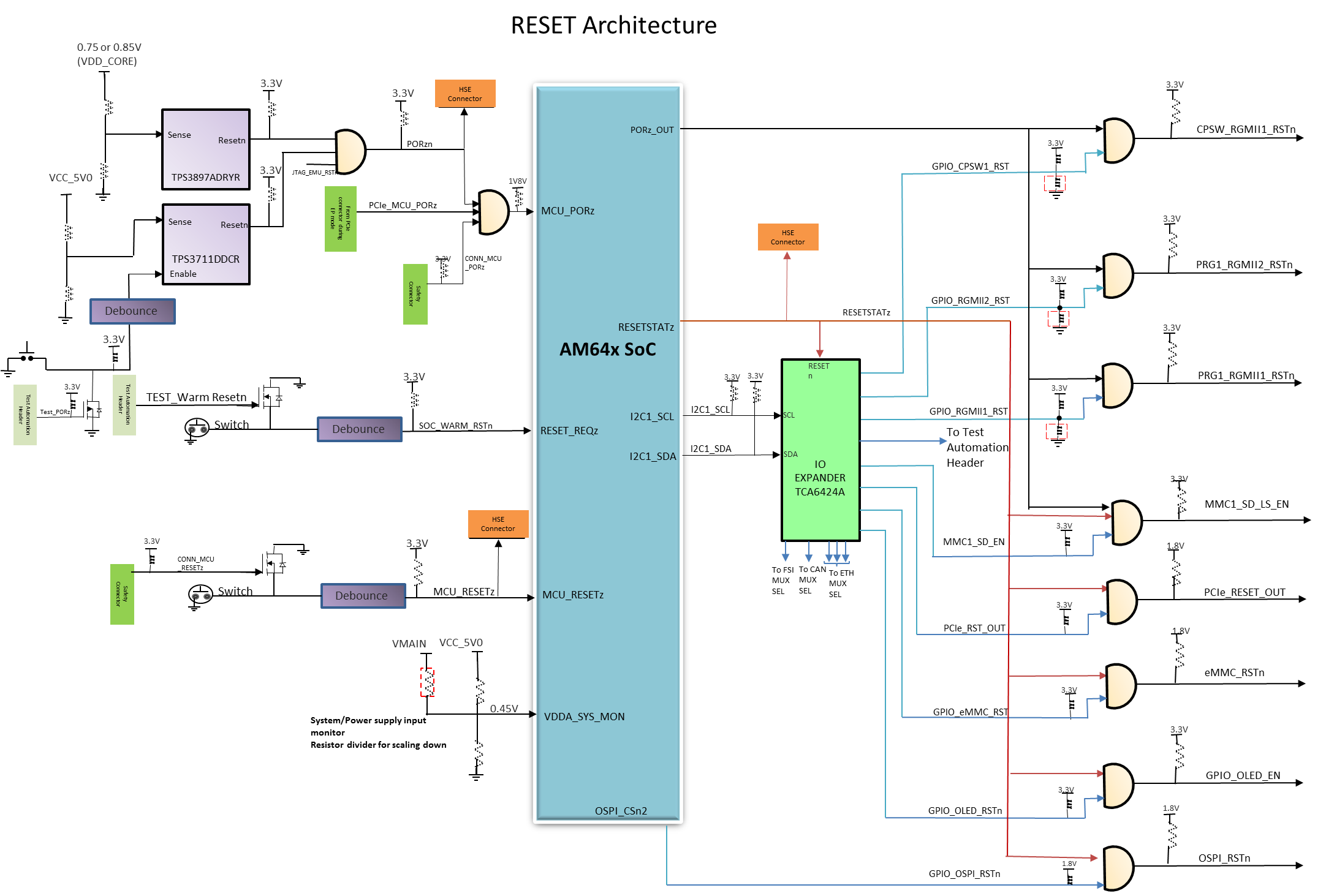
The two supervisor outputs and reset from JTAG are input to an AND gate to generate the PORz signal. This PORz, the CONN_MCU_PORz from safety connector, and PCIe_MCU_PORz from PCIe connector are input to another AND gate to generate the MCU_PORz signal.
Three push button switches are available to provide reset for MCU_PORz, MCU_RESETz and RESET_REQz.
Warm reset can also be applied through Test automation header or manual reset switches SW4(SoC) and SW6(MCU).
MCU_PORz input can be applied though switch SW7.
The CONN_MCU_RESETz and CONN_MCU_PORz from the safety connector are routed to MCU_RESETz and MCU_PORz respectively thereby providing option for safety connector to create a warm reset and a cold reset as shown in the Figure 3-5.
Most peripheral resets are “ANDED” with the RESETSTATz output from the SoC along with a GPIO control as shown in Figure 3-5. This ensures that the peripheral reset is asserted until the SoC is out of reset and allows the AM64x to manually assert reset to the peripheral.
 Figure 3-5 Overall Reset
Architecture of the AM64x/AM243x GP EVM