SPRUIX0D February 2021 – August 2021
- Trademarks
- 1Introduction
- 2Important Usage Notes
-
3System Description
- 3.1 Key Features
- 3.2 Functional Block Diagram
- 3.3 Power-On/Off Procedures
- 3.4
Peripheral and Major Component
Description
- 3.4.1 Clocking
- 3.4.2 Reset
- 3.4.3 Power
- 3.4.4 Configuration
- 3.4.5 JTAG
- 3.4.6 Test Automation
- 3.4.7 UART Interfaces
- 3.4.8 Memory Interfaces
- 3.4.9 Ethernet Interface
- 3.4.10 Display Interface
- 3.4.11 USB 2.0 Interface
- 3.4.12 PCIe Interface
- 3.4.13 High Speed Expansion Interface
- 3.4.14 CAN Interface
- 3.4.15 Interrupt
- 3.4.16 ADC Interface
- 3.4.17 Safety Connector
- 3.4.18 SPI Interfaces
- 3.4.19 I2C Interfaces
- 3.4.20 FSI Interface
- 4Known Issues and Modifications
- 5References
- 6Revision History
3.4.9 Ethernet Interface
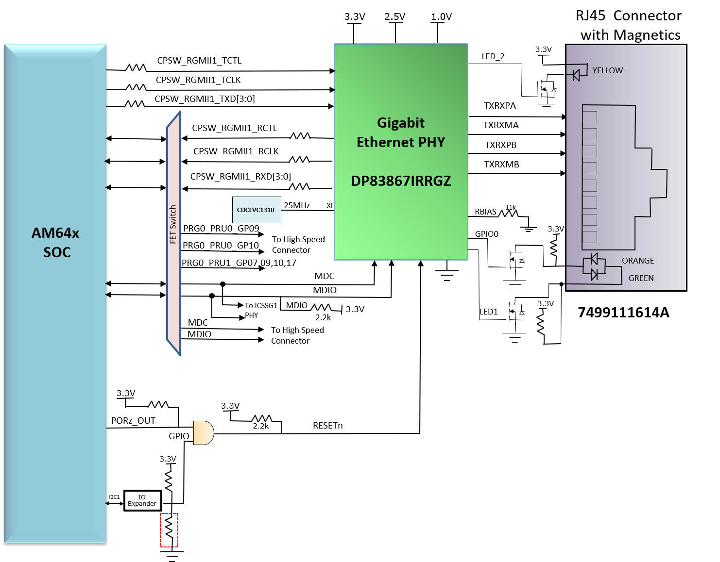
Three Ethernet PHYs terminated to RJ45 connectors with integrated magnetics is supported on the EVM.
 Figure 3-18 Ethernet Interface - CPSW
Domain
Figure 3-18 Ethernet Interface - CPSW
DomainThe first PHY (connected to RJ45 connector J14) is interfaced to the CPSW_RGMII1 port of the SoC. The DP83867 PHY has been selected for this interface based on its ability to configure the Tx and Rx Delays. Since the CPSW_RGMII1_RX port is also multiplexed with PRG0 signals, a mux is needed to select the path from the SoC to this PHY (in CPSW mode) or to the HSE connector (PRG0 mode). The selection is done using a GPIO from the 24 bit IO expander.
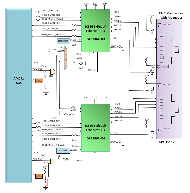
The second PHY (connected to stacked RJ45 connector J21B) is interfaced to the PRG1_RGMII2 port of the SoC. This port is directly multiplexed with the CPSW_RGMII2 port. In order to select between CPSW and PRG operation, we need to multiplex the MDIO MDC signals from each controller to this PHY and the mux shall be controlled by a GPIO from IO expander. PRG1_RGMII2 is also internally multiplexed with PRG1_MII signals. The objective of the PHY used to connect this port is that the PHY should support both RGMII and MII modes, hence DP83869 (48 pin) PHY is selected.
The third PHY (connected to stacked RJ45 connector J21A ) is interfaced to the PRG1_RGMII1 port of the SoC. ICSSG ports support internal multiplexing of GPI, GPO, RGMII, MII etc. The objective of this PHY used to connect to this port is that it should support both RGMII and MII modes (without the use of CRS and COL signals as they are multiplexed with the CPSW_RGMII1 used for the first PHY). Hence the same DP83869 (48pin) PHY is used for this port as well.
 Figure 3-19 Ethernet Interface - ICSSG
Domain