SPRUIX0D February 2021 – August 2021
- Trademarks
- 1Introduction
- 2Important Usage Notes
-
3System Description
- 3.1 Key Features
- 3.2 Functional Block Diagram
- 3.3 Power-On/Off Procedures
- 3.4
Peripheral and Major Component
Description
- 3.4.1 Clocking
- 3.4.2 Reset
- 3.4.3 Power
- 3.4.4 Configuration
- 3.4.5 JTAG
- 3.4.6 Test Automation
- 3.4.7 UART Interfaces
- 3.4.8 Memory Interfaces
- 3.4.9 Ethernet Interface
- 3.4.10 Display Interface
- 3.4.11 USB 2.0 Interface
- 3.4.12 PCIe Interface
- 3.4.13 High Speed Expansion Interface
- 3.4.14 CAN Interface
- 3.4.15 Interrupt
- 3.4.16 ADC Interface
- 3.4.17 Safety Connector
- 3.4.18 SPI Interfaces
- 3.4.19 I2C Interfaces
- 3.4.20 FSI Interface
- 4Known Issues and Modifications
- 5References
- 6Revision History
3.4.4.1 Boot Modes
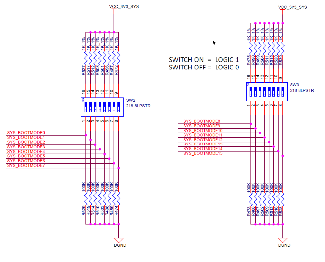
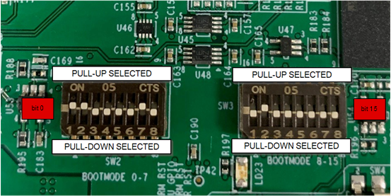
The boot mode for the EVM is defined by either a bank of switches SW2 and SW3 or by the I2C buffer (U96) connected to the test automation connector (J38). All the boot mode pins have a weak pull-down resistor and a switch capable of connecting to a strong pull up resistor. Switch set to “ON” corresponds to logic “HIGH” while “OFF” corresponds to logic “LOW”.
For a full description of all AM64x SoC supported bootmodes, see the AM64x Sitara™ Processors Data Manual and AM64x Processors Silicon Revision 1.0 Texas Instruments Families of Products Technical Reference Manual.
The following boot modes are supported by EVM (and subject to change):
- OSPI
- MMC1 - SD Card
- MMC0 - eMMC installed
- USB - boot using host mode with bulk storage. USB 2.0 mass storage using FAT16/32 (thumb drive)
- USB - device boot DFU
- UART
- No-Boot
 Figure 3-9 AM64x/AM243x GP EVM Schematic Excerpt, Boot Mode Selection Switches
(SW2, SW3)
 Figure 3-10 AM64x/AM243x GP EVP PCB, Boot Mode Selection Switches (SW2,
SW3)
Figure 3-10 AM64x/AM243x GP EVP PCB, Boot Mode Selection Switches (SW2,
SW3)The BOOTMODE pins provide means to select the boot mode before the device is powered up. They are divided into the following categories:
| Bit 15 | Bit 14 | Bit 13 | Bit 12 | Bit 11 | Bit 10 | Bit 9 | Bit 8 | Bit 7 | Bit 6 | Bit 5 | Bit 4 | Bit 3 | Bit 2 | Bit 1 | Bit 0 |
|---|---|---|---|---|---|---|---|---|---|---|---|---|---|---|---|
| RSVD | RSVD | Backup Boot Mode Config | Backup Boot Mode | Primary Boot Mode Config | Primary Boot Mode | PLL Config | |||||||||
BOOTMODE[2:0] - Denote system clock frequency for PLL configuration. By default, these bits are set for 25 MHz.
| SW2.3 | SW2.2 | SW2.1 | PLL REF CLK (MHz) |
|---|---|---|---|
| off | off | off | 19.2 |
| off | off | on | 20 |
| off | on | off | 24 |
| off | on | on | 25 |
| on | off | off | 26 |
| on | off | on | 27 |
| on | on | off | RSVD |
| on | on | on | RSVD |
BOOTMODE[6:3] - This provides primary boot mode configuration to select the requested boot mode after POR, that is, the peripheral/memory to boot from.
| SW2.7 | SW2.6 | SW2.5 | SW2.4 | Primary Boot Device Selected |
|---|---|---|---|---|
| off | off | off | off | RSVD |
| off | off | off | on | OSPI |
| off | off | on | off | QSPI |
| off | off | on | on | SPI |
| off | on | off | off | RSVD |
| off | on | off | on | RSVD |
| off | on | on | off | I2C |
| off | on | on | on | UART |
| on | off | off | off | MMC/SD Card |
| on | off | off | on | eMMC |
| on | off | on | off | USB |
| on | off | on | on | GPMC NAND |
| on | on | off | off | GPMC NOR |
| on | on | off | on | PCIe |
| on | on | on | off | xSPI |
| on | on | on | on | No-boot / Dev-boot |
BOOTMODE[9:7] - These pins provide optional settings and are used in conjunction with the primary boot device selected. For more details, see the device-specific TRM.
| SW3.2 | SW3.1 | SW2.8 | Primary Boot Device |
|---|---|---|---|
| RSVD | RSVD | RSVD | RSVD |
| RSVD | Iclk | Csel | OSPI |
| RSVD | Iclk | Csel | QSPI |
| RSVD | Mode | Csel | SPI |
| RSVD | RSVD | RSVD | RSVD |
| RSVD | RSVD | RSVD | RSVD |
| Bus Reset | Don't Care | Addr | I2C |
| RSVD | RSVD | RSVD | UART |
| Port | RSVD | Fs/raw | MMC / SD Card |
| RSVD | RSVD | RSVD | eMMC |
| Core Volt | Mode | Lane Swap | USB |
| RSVD | RSVD | RSVD | GPMC NAND |
| RSVD | RSVD | RSVD | GPMC NOR |
| RSVD | RSVD | RSVD | PCIe |
| SFDP | Read Cmd | Mode | xSPI |
| RSVD | RSVD | RSVD | No-boot / Dev-boot |
BOOTMODE[12:10] - Select the backup boot mode, that is, the peripheral/memory to boot from, if primary boot device failed.
| SW3.2 | SW3.1 | SW2.8 | Backup Boot Device Selected |
|---|---|---|---|
| off | off | off | None (No backup mode) |
| off | off | on | USB |
| off | on | off | RSVD |
| off | on | on | UART |
| on | off | off | RSVD |
| on | off | on | MMC/SD |
| on | on | off | SPI |
| on | on | on | I2C |
BOOTMODE[13] - These pins provide optional settings and are used in conjunction with the backup boot device devices. For more details on bit details, see the device-specific TRM. When on, switches SW3.6 sets 1 and, when off, sets 0.
| SW3.6 | Boot Device |
|---|---|
| RSVD | None |
| Mode | USB |
| RSVD | RSVD |
| RSVD | UART |
| RSVD | RSVD |
| Port | MMC/SD |
| RSVD | SPI |
| RSVD | I2C |
BOOTMODE[14:15] - Reserved