SLAA530B March 2012 – July 2021 MSP430F5131 , MSP430F5132 , MSP430F5151 , MSP430F5152 , MSP430F5171 , MSP430F5172 , MSP430F5212 , MSP430F5214 , MSP430F5217 , MSP430F5219 , MSP430F5222 , MSP430F5224 , MSP430F5229 , MSP430F5232 , MSP430F5234 , MSP430F5237 , MSP430F5239 , MSP430F5242 , MSP430F5244 , MSP430F5247 , MSP430F5249 , MSP430F5252 , MSP430F5253 , MSP430F5254 , MSP430F5255 , MSP430F5256 , MSP430F5257 , MSP430F5258 , MSP430F5259 , MSP430F5304 , MSP430F5308 , MSP430F5309 , MSP430F5310 , MSP430F5324 , MSP430F5325 , MSP430F5326 , MSP430F5327 , MSP430F5328 , MSP430F5328-EP , MSP430F5329 , MSP430F5333 , MSP430F5335 , MSP430F5336 , MSP430F5338 , MSP430F5340 , MSP430F5341 , MSP430F5342 , MSP430F5358 , MSP430F5359 , MSP430F5418 , MSP430F5418A , MSP430F5419 , MSP430F5419A , MSP430F5435 , MSP430F5435A , MSP430F5436 , MSP430F5436A , MSP430F5437 , MSP430F5437A , MSP430F5438 , MSP430F5438A , MSP430F5438A-EP , MSP430F5500 , MSP430F5501 , MSP430F5502 , MSP430F5503 , MSP430F5504 , MSP430F5505 , MSP430F5506 , MSP430F5507 , MSP430F5508 , MSP430F5509 , MSP430F5510 , MSP430F5513 , MSP430F5514 , MSP430F5515 , MSP430F5517 , MSP430F5519 , MSP430F5521 , MSP430F5522 , MSP430F5524 , MSP430F5525 , MSP430F5526 , MSP430F5527 , MSP430F5528 , MSP430F5529 , MSP430F5630 , MSP430F5631 , MSP430F5632 , MSP430F5633 , MSP430F5634 , MSP430F5635 , MSP430F5636 , MSP430F5637 , MSP430F5638 , MSP430F5658 , MSP430F5659 , MSP430F6433 , MSP430F6435 , MSP430F6436 , MSP430F6438 , MSP430F6458 , MSP430F6459 , MSP430F6459-HIREL , MSP430F6630 , MSP430F6631 , MSP430F6632 , MSP430F6633 , MSP430F6634 , MSP430F6635 , MSP430F6636 , MSP430F6637 , MSP430F6638 , MSP430F6658 , MSP430F6659 , MSP430F6720 , MSP430F6720A , MSP430F6721 , MSP430F6721A , MSP430F6723 , MSP430F6723A , MSP430F6724 , MSP430F6724A , MSP430F6725 , MSP430F6725A , MSP430F6726 , MSP430F6726A , MSP430F6730 , MSP430F6730A , MSP430F6731 , MSP430F6731A , MSP430F6733 , MSP430F6733A , MSP430F6734 , MSP430F6734A , MSP430F6735 , MSP430F6735A , MSP430F6736 , MSP430F6736A , MSP430F6745 , MSP430F67451 , MSP430F67451A , MSP430F6745A , MSP430F6746 , MSP430F67461 , MSP430F67461A , MSP430F6746A , MSP430F6747 , MSP430F67471 , MSP430F67471A , MSP430F6747A , MSP430F6748 , MSP430F67481 , MSP430F67481A , MSP430F6748A , MSP430F6749 , MSP430F67491 , MSP430F67491A , MSP430F6749A , MSP430F67621 , MSP430F67621A , MSP430F67641 , MSP430F67641A , MSP430F6765 , MSP430F67651 , MSP430F67651A , MSP430F6765A , MSP430F6766 , MSP430F67661 , MSP430F67661A , MSP430F6766A , MSP430F6767 , MSP430F67671 , MSP430F67671A , MSP430F6767A , MSP430F6768 , MSP430F67681 , MSP430F67681A , MSP430F6768A , MSP430F6769 , MSP430F67691 , MSP430F67691A , MSP430F6769A , MSP430F6775 , MSP430F67751 , MSP430F67751A , MSP430F6775A , MSP430F6776 , MSP430F67761 , MSP430F67761A , MSP430F6776A , MSP430F6777 , MSP430F67771 , MSP430F67771A , MSP430F6777A , MSP430F6778 , MSP430F67781 , MSP430F67781A , MSP430F6778A , MSP430F6779 , MSP430F67791 , MSP430F67791A , MSP430F6779A , MSP430FR2000 , MSP430FR2032 , MSP430FR2033 , MSP430FR2100 , MSP430FR2110 , MSP430FR2111 , MSP430FR2153 , MSP430FR2155 , MSP430FR2310 , MSP430FR2311 , MSP430FR2353 , MSP430FR2355 , MSP430FR2422 , MSP430FR2433 , MSP430FR2475 , MSP430FR2476 , MSP430FR2512 , MSP430FR2522 , MSP430FR2532 , MSP430FR2533 , MSP430FR2632 , MSP430FR2633 , MSP430FR2672 , MSP430FR2673 , MSP430FR2675 , MSP430FR2676 , MSP430FR4131 , MSP430FR4132 , MSP430FR4133 , MSP430FR5041 , MSP430FR5043 , MSP430FR50431 , MSP430FR5720 , MSP430FR5721 , MSP430FR5722 , MSP430FR5723 , MSP430FR5724 , MSP430FR5725 , MSP430FR5726 , MSP430FR5727 , MSP430FR5728 , MSP430FR5729 , MSP430FR5730 , MSP430FR5731 , MSP430FR5732 , MSP430FR5733 , MSP430FR5734 , MSP430FR5735 , MSP430FR5736 , MSP430FR5737 , MSP430FR5738 , MSP430FR5739 , MSP430FR5739-EP , MSP430FR5847 , MSP430FR58471 , MSP430FR5848 , MSP430FR5849 , MSP430FR5857 , MSP430FR5858 , MSP430FR5859 , MSP430FR5867 , MSP430FR58671 , MSP430FR5868 , MSP430FR5869 , MSP430FR5870 , MSP430FR5872 , MSP430FR58721 , MSP430FR5887 , MSP430FR5888 , MSP430FR5889 , MSP430FR58891 , MSP430FR5922 , MSP430FR59221 , MSP430FR5947 , MSP430FR59471 , MSP430FR5948 , MSP430FR5949 , MSP430FR5957 , MSP430FR5958 , MSP430FR5959 , MSP430FR5962 , MSP430FR5964 , MSP430FR5967 , MSP430FR5968 , MSP430FR5969 , MSP430FR5969-SP , MSP430FR59691 , MSP430FR5970 , MSP430FR5972 , MSP430FR59721 , MSP430FR5986 , MSP430FR5987 , MSP430FR5988 , MSP430FR5989 , MSP430FR5989-EP , MSP430FR59891 , MSP430FR5992 , MSP430FR5994 , MSP430FR59941 , MSP430FR6005 , MSP430FR6007 , MSP430FR6035 , MSP430FR6037 , MSP430FR60371 , MSP430FR6041 , MSP430FR6043 , MSP430FR60431 , MSP430FR6045 , MSP430FR6047 , MSP430FR60471 , MSP430FR6820 , MSP430FR6822 , MSP430FR68221 , MSP430FR6870 , MSP430FR6872 , MSP430FR68721 , MSP430FR6877 , MSP430FR6879 , MSP430FR68791 , MSP430FR6887 , MSP430FR6888 , MSP430FR6889 , MSP430FR68891 , MSP430FR6920 , MSP430FR6922 , MSP430FR69221 , MSP430FR6927 , MSP430FR69271 , MSP430FR6928 , MSP430FR6970 , MSP430FR6972 , MSP430FR69721 , MSP430FR6977 , MSP430FR6979 , MSP430FR69791 , MSP430FR6987 , MSP430FR6988 , MSP430FR6989 , MSP430FR69891
- Trademarks
- 1Introduction to ESD
- 2General System-Level ESD Design Guidelines
- 3System Efficient ESD Design (SEED)
- 4SEED-Based IEC Protection Design and Verification – Real World Example 1
- 5System-Level ESD Protection – Real World Example 2
- 6Summary
- 7Modeling Using TLP Parameters
- 8References
- Revision History
2.2 PCB Design and Layout
Good PCB design and layout can be extremely effective in suppressing ESD in the system. These are general guidelines for ESD- and EMI-immune PCB layout:
- Use ground planes instead of ground traces where possible to lower the current-path inductance.
- Use multipoint and thicker grounds where you want ESD currents to flow, and single-point and thinner grounds where you don't.
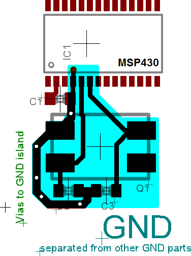
- If it is not practicable to create a continuous ground plane by using copper pour in the layout, then create smaller copper pour sections that are in turn connected to the rest of the ground. However, do not create isolated copper pour islands; they can induce noise and arc in presence of ESD.
- If possible, use multi-layer PCBs with paired power and ground planes.
- If possible, place solid or filled vias into power and ground planes. These vias provide excellent thermal dissipation in case of an ESD event and also ensure good electrical and power supply connections. For the plated through-hole components, use thermal vias.
- Keep traces as short as possible to reduce trace inductance.
- Avoid routing traces at right angles to component pins or other traces. Right angle traces
should be avoided as they are known to cause more radiation. This becomes more critical in high-speed designs.
 Figure 2-5 Avoid Right-Angle Traces
 - Keep sensitive signal traces away from PCB edges.
- Place all connectors and external wires on one edge of the PCB.
- Place ESD susceptible circuitry at the center of the PCB (away from the edges of the board, external wires, connectors and power).
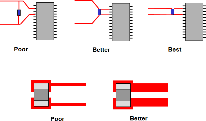
- Decoupling (see Figure 2-6)
- Use decoupling capacitors with low effective series resistance (ESR) and effective series inductance (ESL) to decouple the IC (MSP430 in this case) power from the rest of the supply system.
- Place the decoupling capacitor close to the IC power pins.
- Keep the traces from decoupling caps to GND as short (and thick) as possible.
 Figure 2-6 Decoupling Basics
 - Crystal layout
Crystal connections on PCB layout are very important as crystals are susceptible to ESD and EMI noise in the system. Poor designs can cause the crystal to dropout or cause jitter in the crystal oscillator clock. These are general guidelines for ESD-immune PCB layout practices:
- Crystal should be placed as close to the MSP430 as possible
- The traces connecting the crystal should be short and direct
- Ensure no traces run beneath the crystal
- Keep switching signals away from the crystal layout to avoid causing crystal dropout (see Section 5 for real world example based on this)
- Keep a clean ground plane beneath the crystal
- Ground the crystal can as well; use guard rings around the leads
Figure 2-7 shows an example crystal layout that follows all of these design recommendations.
 Figure 2-7 Example Crystal Layout
This topic is discussed in greater detail in the MSP430 32-kHz Crystal Oscillator application note) [11].
- Current Loops
An electrical circuit is always a closed loop. Every signal path has a return path back to the source; also called the return current. With DC, the return current takes the lowest resistance path back. With higher frequency, the return current flows along the lowest impedance; that is directly beneath the forward signal path [12]. Current loops in the layout generate noise and should be minimized by keeping forward and return currents together. It helps both EMI and ESD performance. Solid ground plane provides continuous, low-impedance path for return current.
- For a two-layer board, try to dedicate one layer as mostly solid ground plane, with routing slots cut out for signal traces
- Figure 2-8 shows a solid ground plane.
Only breaks in the plane are vias and through-holes. This is the ideal case.
 Figure 2-8 Example Layout With Solid Ground Plane
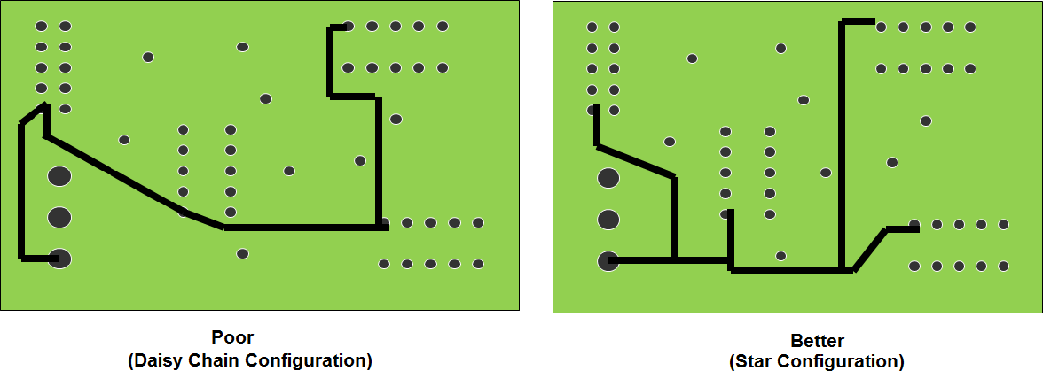
 - If one of the layers cannot be dedicated as ground plane, then use a star configuration
instead of a daisy chain configuration to connect all grounds. Daisy chaining forces all the signals to follow the same return path
possibly causing ground bounce.
 Figure 2-9 Grounding Considerations For 2-Layer Board With No Dedicated
Ground Plane
 - Make sure that no traces on the other layer perpendicularly cross a break or slot in the
ground plane. Otherwise, it forms a large inductive loop that can generate and pick up noise. If the return path, particularly the
ground plane, has a break or slot, the return current must take a different route, and this results in a loop area (see Figure 2-10(a)). The larger the loop area,
the more radiation and EMI problems occur.
 Figure 2-10 Return Currents and Resulting Loop Area
 - The designer must make sure that the return current flows directly underneath the signal trace. One way is to physically connect the areas separated by the slot (for example, by placing a 0-Ω resistor over the slot) Figure 2-10(b). Another way is to route the signal same way as the return current flows Figure 2-10(c) [12]. This is also the best way here.
- Keep loop areas between power and ground as small as possible (see Section 2.2.1 for example layout discussion illustrating this).
- Keep loop areas of switching signals as small as possible.
- Keep loop area of oscillator signals as small as possible.