SLUA887A August 2018 – September 2023 LM2005 , LM2101 , LM2103 , LM2104 , LM2105 , LM25101 , LM27222 , LM2724A , LM5100A , LM5100B , LM5100C , LM5101 , LM5101A , LM5101B , LM5101C , LM5102 , LM5104 , LM5105 , LM5106 , LM5107 , LM5108 , LM5109 , LM5109A , LM5109B , LM5109B-Q1 , LM5113-Q1 , LMG1205 , LMG1210 , SM72295 , SM74104 , TPS28225 , TPS28225-Q1 , TPS28226 , TPS2832 , TPS2836 , TPS2837 , UC2950 , UCC27200 , UCC27200-Q1 , UCC27200A , UCC27201 , UCC27201A , UCC27201A-DIE , UCC27201A-Q1 , UCC27211 , UCC27211A , UCC27211A-Q1 , UCC27212 , UCC27212A-Q1 , UCC27222 , UCC27282 , UCC27282-Q1 , UCC27284 , UCC27284-Q1 , UCC27288 , UCC27289 , UCC27301A , UCC27301A-Q1 , UCC27302A , UCC27302A-Q1 , UCC27311A , UCC27311A-Q1 , UCC27710 , UCC27712 , UCC27712-Q1 , UCC27714
2 Basic Operation of Bootstrap Circuit
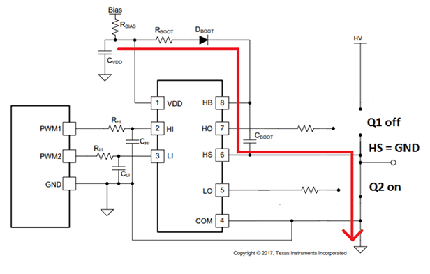
A bootstrap circuit is used in half-bridge configurations to supply bias to the high-side FET. Figure 2-1 shows the charging path of a bootstrap circuit in a simplified half-bridge configuration using UCC27710, TI's 620V half-bridge driver with interlock. When the low-side FET is on (high-side FET is off), the HS pin and the switch node are pulled to ground; the VDD bias supply, through the bypass capacitor, charges the bootstrap capacitor through the bootstrap diode and resistor.
 Figure 2-1 Bootstrap Charging
Path
Figure 2-1 Bootstrap Charging
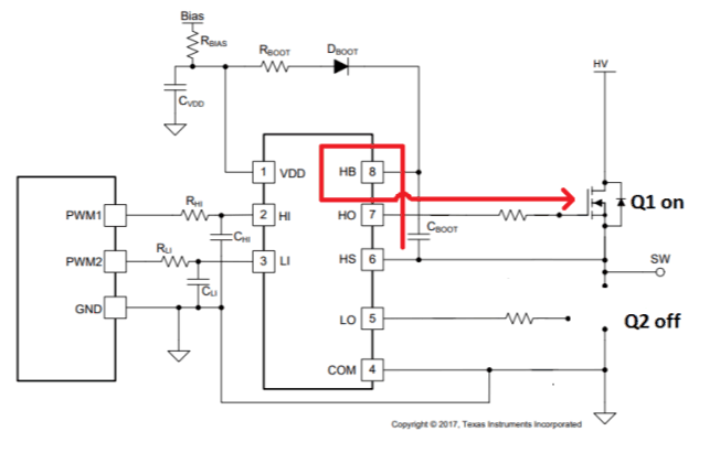
PathWhen the low-side FET is turned off and the high-side is on, the HS pin of the gate driver and the switch node are pulled to the high voltage bus HV; the bootstrap capacitor discharges some of the stored voltage (accumulated during the charging sequence) to the high-side FET through the HO and HS pins of the gate driver as shown in Figure 2-2.
 Figure 2-2 Bootstrap Capacitor
Discharging Path