SLVA959B November 2018 – October 2021 DRV10866 , DRV10963 , DRV10964 , DRV10970 , DRV10974 , DRV10975 , DRV10983 , DRV10983-Q1 , DRV10987 , DRV11873 , DRV3205-Q1 , DRV3220-Q1 , DRV3245E-Q1 , DRV3245Q-Q1 , DRV8301 , DRV8302 , DRV8303 , DRV8304 , DRV8305 , DRV8305-Q1 , DRV8306 , DRV8307 , DRV8308 , DRV8312 , DRV8313 , DRV8320 , DRV8320R , DRV8323 , DRV8323R , DRV8332 , DRV8343-Q1 , DRV8350 , DRV8350R , DRV8353 , DRV8353R , DRV8412 , DRV8701 , DRV8702-Q1 , DRV8702D-Q1 , DRV8703-Q1 , DRV8703D-Q1 , DRV8704 , DRV8711 , DRV8800 , DRV8801 , DRV8801-Q1 , DRV8801A-Q1 , DRV8802 , DRV8802-Q1 , DRV8803 , DRV8804 , DRV8805 , DRV8806 , DRV8811 , DRV8812 , DRV8813 , DRV8814 , DRV8816 , DRV8818 , DRV8821 , DRV8823 , DRV8823-Q1 , DRV8824 , DRV8824-Q1 , DRV8825 , DRV8828 , DRV8829 , DRV8830 , DRV8832 , DRV8832-Q1 , DRV8833 , DRV8833C , DRV8834 , DRV8835 , DRV8836 , DRV8837 , DRV8837C , DRV8838 , DRV8839 , DRV8840 , DRV8841 , DRV8842 , DRV8843 , DRV8844 , DRV8846 , DRV8847 , DRV8848 , DRV8850 , DRV8860 , DRV8870 , DRV8871 , DRV8871-Q1 , DRV8872 , DRV8872-Q1 , DRV8873-Q1 , DRV8880 , DRV8881 , DRV8884 , DRV8885 , DRV8886 , DRV8886AT , DRV8889-Q1
2.4 Thermal Via Connections
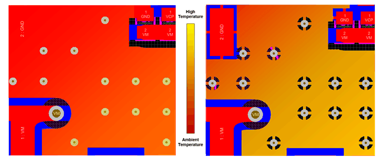
Thermal vias should connect the top and bottom layers together so heat can dissipate from the IC onto both layers. Thermal relief connections should not be used for thermal vias because the path for heat to flow from the top plane through the via to the bottom plane is constricted. This constricted path for heat flow results in an increased temperature on the remaining part of the top plane around the via. Directly connecting vias allows for the lowest possible thermal resistance between the via and copper layers. The thermal vias should make their connection to the internal ground plane with a complete connection around the entire circumference of the plated through hole. Do not cover the vias with solder mask which causes excessive voiding. Figure 2-3 shows temperature differences between thermal relief and direct-connect vias.
 Figure 2-3 Thermal Relief vs Direct-Connect Heat Map
Thermal relief joints connect planes with vias or components electrically, but they reduce the flow of heat between the component or via and the plane. This is done so a soldering iron or reflow oven only heats the component and ensures a reliable solder connection. This method can be effective for applications where the vias are not required for thermal conduction between planes. However, power applications, such as motor drivers, require that these vias be directly bonded to the plane for optimal thermal performance between layers.