SLVA959B November 2018 – October 2021 DRV10866 , DRV10963 , DRV10964 , DRV10970 , DRV10974 , DRV10975 , DRV10983 , DRV10983-Q1 , DRV10987 , DRV11873 , DRV3205-Q1 , DRV3220-Q1 , DRV3245E-Q1 , DRV3245Q-Q1 , DRV8301 , DRV8302 , DRV8303 , DRV8304 , DRV8305 , DRV8305-Q1 , DRV8306 , DRV8307 , DRV8308 , DRV8312 , DRV8313 , DRV8320 , DRV8320R , DRV8323 , DRV8323R , DRV8332 , DRV8343-Q1 , DRV8350 , DRV8350R , DRV8353 , DRV8353R , DRV8412 , DRV8701 , DRV8702-Q1 , DRV8702D-Q1 , DRV8703-Q1 , DRV8703D-Q1 , DRV8704 , DRV8711 , DRV8800 , DRV8801 , DRV8801-Q1 , DRV8801A-Q1 , DRV8802 , DRV8802-Q1 , DRV8803 , DRV8804 , DRV8805 , DRV8806 , DRV8811 , DRV8812 , DRV8813 , DRV8814 , DRV8816 , DRV8818 , DRV8821 , DRV8823 , DRV8823-Q1 , DRV8824 , DRV8824-Q1 , DRV8825 , DRV8828 , DRV8829 , DRV8830 , DRV8832 , DRV8832-Q1 , DRV8833 , DRV8833C , DRV8834 , DRV8835 , DRV8836 , DRV8837 , DRV8837C , DRV8838 , DRV8839 , DRV8840 , DRV8841 , DRV8842 , DRV8843 , DRV8844 , DRV8846 , DRV8847 , DRV8848 , DRV8850 , DRV8860 , DRV8870 , DRV8871 , DRV8871-Q1 , DRV8872 , DRV8872-Q1 , DRV8873-Q1 , DRV8880 , DRV8881 , DRV8884 , DRV8885 , DRV8886 , DRV8886AT , DRV8889-Q1
2.1 PCB Conduction and Convection
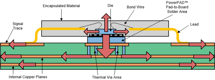
An important consideration for motor driver thermal performance is the pathways which heat generated inside the device can dissipate. Three primary paths for heat to go from the die into lower temperature environments are:
- Encapsulation material
- Bond wires
- Thermal pad
Using these three paths as examples, the thermal pad is the most efficient path for heat to go from the device, followed by the encapsulation material, and finally the bond wires. The technology used in the thermal pad integrated circuit package creates a low thermally resistive path from the die to external copper planes. Therefore the thermal pad can efficiently conduct a large amount of heat away from the die. The thermal pad poured underneath the driver should be large enough to cover the entire area of the thermal pad, and still include a large surface area on other parts of the PCB. The thermal pad should also be tightly bound to the bottom ground plane with several thermal vias placed directly underneath the thermal pad. Figure 2-1 shows an example of the exit paths used by heat generated in the device die.
 Figure 2-1 Cross Section of Thermal Pad™ Package Mounted to PCB and Resulting Heat Transfer
Connecting both the top and bottom ground planes to the thermal pad of the driver significantly improves the amount of heat dissipated in a PCB design. For this reason, these planes should be made as large as possible in the layout.