SLVA959B November 2018 – October 2021 DRV10866 , DRV10963 , DRV10964 , DRV10970 , DRV10974 , DRV10975 , DRV10983 , DRV10983-Q1 , DRV10987 , DRV11873 , DRV3205-Q1 , DRV3220-Q1 , DRV3245E-Q1 , DRV3245Q-Q1 , DRV8301 , DRV8302 , DRV8303 , DRV8304 , DRV8305 , DRV8305-Q1 , DRV8306 , DRV8307 , DRV8308 , DRV8312 , DRV8313 , DRV8320 , DRV8320R , DRV8323 , DRV8323R , DRV8332 , DRV8343-Q1 , DRV8350 , DRV8350R , DRV8353 , DRV8353R , DRV8412 , DRV8701 , DRV8702-Q1 , DRV8702D-Q1 , DRV8703-Q1 , DRV8703D-Q1 , DRV8704 , DRV8711 , DRV8800 , DRV8801 , DRV8801-Q1 , DRV8801A-Q1 , DRV8802 , DRV8802-Q1 , DRV8803 , DRV8804 , DRV8805 , DRV8806 , DRV8811 , DRV8812 , DRV8813 , DRV8814 , DRV8816 , DRV8818 , DRV8821 , DRV8823 , DRV8823-Q1 , DRV8824 , DRV8824-Q1 , DRV8825 , DRV8828 , DRV8829 , DRV8830 , DRV8832 , DRV8832-Q1 , DRV8833 , DRV8833C , DRV8834 , DRV8835 , DRV8836 , DRV8837 , DRV8837C , DRV8838 , DRV8839 , DRV8840 , DRV8841 , DRV8842 , DRV8843 , DRV8844 , DRV8846 , DRV8847 , DRV8848 , DRV8850 , DRV8860 , DRV8870 , DRV8871 , DRV8871-Q1 , DRV8872 , DRV8872-Q1 , DRV8873-Q1 , DRV8880 , DRV8881 , DRV8884 , DRV8885 , DRV8886 , DRV8886AT , DRV8889-Q1
1.4 EMC Considerations
The electromagnetic compatibility (EMC) primarily depends on the layout and the electrical connection between the components.
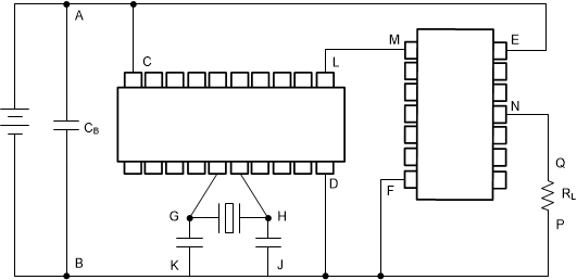
The return path of each signal must flow from the resource to the signal origin which creates current loops. This line loop creates an antenna that can radiate electromagnetic energy which is determined by the current amplitude, the repetition frequency of the signal, and the geometrical area of the current loops. It is recommended to minimize these current loops for optimal EMC performance, Figure 1-6 shows common types of current loops.
 Figure 1-6 Current Paths in an Electronic System
The supply lines in Figure 1-6 form loops A–C–D–B and A–E–F–B. The energy that the system requires to operate is conducted by these lines.
Loops L-M-F-D, N-Q-P-F, and G-H-J-K are formed by signals and controls. The area these lines enclose is usually small if those lines outside the system are not considered. However, these lines must be considered at high frequency because they often transmit signals which can affect EMC performance.
Current loops can also form when connectors, headers, or other components break up a ground plane. This causes high-frequency components of switching currents to travel further around the board and effectively create a large loop. This can also occur with vias and is highlighted in Section 3.2.2