SLVA959B November 2018 – October 2021 DRV10866 , DRV10963 , DRV10964 , DRV10970 , DRV10974 , DRV10975 , DRV10983 , DRV10983-Q1 , DRV10987 , DRV11873 , DRV3205-Q1 , DRV3220-Q1 , DRV3245E-Q1 , DRV3245Q-Q1 , DRV8301 , DRV8302 , DRV8303 , DRV8304 , DRV8305 , DRV8305-Q1 , DRV8306 , DRV8307 , DRV8308 , DRV8312 , DRV8313 , DRV8320 , DRV8320R , DRV8323 , DRV8323R , DRV8332 , DRV8343-Q1 , DRV8350 , DRV8350R , DRV8353 , DRV8353R , DRV8412 , DRV8701 , DRV8702-Q1 , DRV8702D-Q1 , DRV8703-Q1 , DRV8703D-Q1 , DRV8704 , DRV8711 , DRV8800 , DRV8801 , DRV8801-Q1 , DRV8801A-Q1 , DRV8802 , DRV8802-Q1 , DRV8803 , DRV8804 , DRV8805 , DRV8806 , DRV8811 , DRV8812 , DRV8813 , DRV8814 , DRV8816 , DRV8818 , DRV8821 , DRV8823 , DRV8823-Q1 , DRV8824 , DRV8824-Q1 , DRV8825 , DRV8828 , DRV8829 , DRV8830 , DRV8832 , DRV8832-Q1 , DRV8833 , DRV8833C , DRV8834 , DRV8835 , DRV8836 , DRV8837 , DRV8837C , DRV8838 , DRV8839 , DRV8840 , DRV8841 , DRV8842 , DRV8843 , DRV8844 , DRV8846 , DRV8847 , DRV8848 , DRV8850 , DRV8860 , DRV8870 , DRV8871 , DRV8871-Q1 , DRV8872 , DRV8872-Q1 , DRV8873-Q1 , DRV8880 , DRV8881 , DRV8884 , DRV8885 , DRV8886 , DRV8886AT , DRV8889-Q1
4 General Routing Techniques
Follow these general routing techniques when doing a motor driver PCB design:
- Make gate drive traces wide and as short in length as possible. Start with a trace width of 20 mils for at least a 1 oz copper, more if required by high currents.
 Figure 4-1 DRV8323xEVM Gate Signal
 - Route the signal trace of the high-side gate and the switch node trace as close as possible to minimize inductance, loop area, and the possibility of noise caused by dv/dt switching.
 Figure 4-2 Parallel Gate Traces
 - Do not use right-angle traces. A 90 degree bend in a trace an acts as an impedance and can cause the current to reflect. When the phases of the motor are switching, the sharp bends can introduce electromagnetic interference (EMI) issues. Circular bends are ideal but may not be practical in actual designs. The best practice for corner routing is to use obtuse angles. Figure 4-3 shows different examples of angles in traces.
 Figure 4-3 Right Angle Trace
 - Transition vias to pads, specifically from thin to thick traces on the output pins. The teardrop technique decreases the thermal stress of the signal transition. This technique also avoids crack of the traces and makes the trace more robust mechanically. The teardrop technique is applicable when going from a small signal to a through-hole pad.
 Figure 4-4 Transitioning Vias to Pads
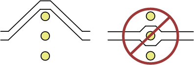
 - Route traces in parallel pairs when routing around an object to avoid differential impedance and discontinuities caused by split traces. This method is important for the signals of the current sense amplifiers.
 Figure 4-5 Routing Parallel Traces
 - Place passive components within the signal path, such as source-matching resistors or ac-coupling capacitors, and next to each other. Placing components in parallel creates wider traces spacing. Staggering components is not recommended as it creates narrow areas.
 Figure 4-6 Recommended Component Placing
 - Separate grounding for analog and digital portions of circuitry is one of the simplest and most effective methods of noise suppression.
 Figure 4-7 Analog and Digital Ground Separation