SLLA472A March 2020 – February 2022 ISO5852S , ISO5852S-EP , ISO5852S-Q1 , LM2005 , LM2101 , LM2103 , LM2104 , LM2105 , LM25101 , LM27222 , LM2724A , LM5100A , LM5100B , LM5100C , LM5101 , LM5101A , LM5101B , LM5101C , LM5102 , LM5104 , LM5105 , LM5106 , LM5107 , LM5108 , LM5109 , LM5109A , LM5109B , LM5109B-Q1 , LM5113-Q1 , LMG1205 , LMG1210 , SM72295 , SM74104 , TPS28225 , TPS28225-Q1 , TPS28226 , TPS2832 , TPS2836 , TPS2837 , UC2950 , UCC27200 , UCC27200-Q1 , UCC27200A , UCC27201 , UCC27201A , UCC27201A-DIE , UCC27201A-Q1 , UCC27211 , UCC27211A , UCC27211A-Q1 , UCC27212 , UCC27212A-Q1 , UCC27222 , UCC27282 , UCC27282-Q1 , UCC27284 , UCC27284-Q1 , UCC27288 , UCC27289 , UCC27301A , UCC27301A-Q1 , UCC27311A , UCC27311A-Q1 , UCC27710 , UCC27712 , UCC27712-Q1 , UCC27714 , UCC27734 , UCC27734-Q1 , UCC27735 , UCC27735-Q1 , UCC27834 , UCC27834-Q1 , UCC27884 , UCC27884-Q1
2 Current Boost With BJT Totem Pole Stage
The most common current-boosting method is the use of an NPN-PNP transistor pair. The gate-drive output from the integrated driver is applied as the base drive for this transistor pair. Figure 2-1 shows the schematic of such a current boost circuit using the isolated gate-driver ISO5852S.
 Figure 2-1 High-Current Gate Driver Using ISO5852S and
BJTs
Figure 2-1 High-Current Gate Driver Using ISO5852S and
BJTsSignal isolation for the PWM input from MCU is provided by the driver IC itself. The gate-driver IC provides an isolation of 5.7 kVRMS and can source and sink 2.5 and 5 A of current, respectively. Power isolation is achieved by an isolated flyback power supply built around the LM5180 device, a primary side regulated flyback converter with integrated 100-V MOSFET. For input side to output side isolation, a flyback transformer from Wurth Elektronik (part no: 750344600) is used. The use of this controller allows this gate-driver circuit to be compatible with 24-, 15-, or 12-V auxiliary power supplies. The primary (MCU) side of the ISO5852S can either be powered using the MCU power supply itself (by depopulating U3 and connecting the MCU supply to 3V3_MCU input), or by a 5-V supply generated by a TLV70450 LDO from the auxiliary power source. The gate-drive power generated by the flyback power stage is suitable for both IGBTs and SiC MOSFETs, as it is has dual outputs of +20 V and –6 V. The RST and PWM signals are from the MCU – PWM is the drive signal and RST (active low) is used for resetting the gate driver after clearing a fault event due to the DESAT pin detecting a short circuit of the power switch. About 10-ns noise filtering is provided on the PWM input. The FLT and RDY signals are status indication signals back to the MCU – FLT indicating by active low a fault situation detected by the gate driver and RDY indicating by active high that the driver is ready to receive PWM input.
On the output side, the NPN and PNP totem pole stage does current amplification. The BJTs that were used for current amplification were PHPT60410NYX and PHPT60410PYX, with a 20-A peak current rating. Because of the use of transistors in the active region, the drive outputs will be reduced by 0.7 V–0.8 V from the power-supply rails. This is not a significant problem with such high drive voltages. Also, adding a resistor between the base and emitter of the external transistors will allow the output voltage to reach the rail voltages. The ISO5852S device has an internal Miller clamp capable of sinking 2.5 A, typical. This pin can also be configured to drive an external PNP transistor for an external clamp. Using an external clamp increases the effectiveness by positioning it much closer to the gate of the power switch. With a sufficiently high negative bias of –6 V, it is not essential to use the Miller clamp, but is included as additional safety and also for demonstration of current boosting of the Miller clamp output. The diodes in D4 protect the output transistors from overvoltage during transient situations.
The DESAT overcurrent protection function in ISO5852S is maintained in this gate driver without any change from the recommended sensing circuit. However, due to the current boosting on the output drive, the slow turn-off DESAT protection might not work well without some modification of the circuit. The R16 – C20 network will ensure that the drive current during a DESAT event will be diverted away from the base of Q2 for the required amount of turn-off time. The values of these components can be calculated using Equation 1 and Equation 2:
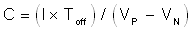
where
- I is the value of the internal current source which is 130 mA
- Toff is the desired turn-off time
- VP is the positive drive voltage
- VN is the negative drive voltage
The value of R16 can be estimated using the inequality in Equation 2: