SPRAAR7J November 2018 – February 2023 66AK2G12 , AM1806 , AM1808 , AM2431 , AM2432 , AM2434 , AM3351 , AM3352 , AM3354 , AM3356 , AM3357 , AM3358 , AM3358-EP , AM3359 , AM3871 , AM3874 , AM3892 , AM3894 , AM4376 , AM4377 , AM4378 , AM4379 , AM5706 , AM5708 , AM5716 , AM5718 , AM5726 , AM5728 , AM5729 , AM5746 , AM5748 , AM5749 , AM620-Q1 , AM623 , AM625 , AM625-Q1 , AM625SIP , AM62A1-Q1 , AM62A3 , AM62A3-Q1 , AM62A7 , AM62A7-Q1 , AM62P , AM62P-Q1 , AM6411 , AM6412 , AM6421 , AM6422 , AM6441 , AM6442 , AM6526 , AM6528 , AM6546 , AM6548 , BQ24392-Q1 , HD3SS6126 , LP8727 , OMAP-L137 , OMAP5912 , TMS320C6745 , TMS320DM355 , TMS320DM365 , TMS320DM368 , TMS320DM369 , TMS320DM6441 , TMS320DM6443 , TMS320DM6446 , TMS320DM6467 , TMS320DM8127 , TMS320DM8147 , TMS320DM8148 , TMS320DM8165 , TMS320DM8167 , TMS320DM8168 , TMS320VC5506 , TMS320VC5507 , TMS320VC5509A , TS3USB221A-Q1 , TS3USBA225 , TSU5511 , TSU5611 , TSU6111 , TSU6111A , TSU6721 , TSU8111
- Abstract
- Trademarks
- 1Introduction
- 2General High-Speed Signal Routing
-
3High-Speed Differential Signal Routing
- 3.1 Differential Signal Spacing
- 3.2 High-Speed Differential Signal Rules
- 3.3 Symmetry in the Differential Pairs
- 3.4 Crosstalk Between the Differential Signal Pairs
- 3.5 Connectors and Receptacles
- 3.6 Via Discontinuity Mitigation
- 3.7 Back-Drill Stubs
- 3.8 Increase Via Anti-Pad Diameter
- 3.9 Equalize Via Count
- 3.10 Surface-Mount Device Pad Discontinuity Mitigation
- 3.11 Signal Bending
- 3.12 Suggested PCB Stackups
- 3.13 ESD/EMI Considerations
- 3.14 ESD/EMI Layout Rules
- 4References
- A Device Layout Parameters
- Revision History
3.6 Via Discontinuity Mitigation
A via presents a short section of change in geometry to a trace and can appear as a capacitive and/or an inductive discontinuity. These discontinuities result in reflections and some degradation of a signal as it travels through the via. Reduce the overall via stub length to minimize the negative impacts of vias (and associated via stubs).
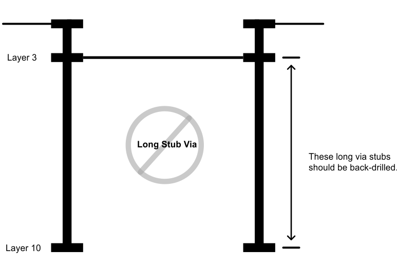
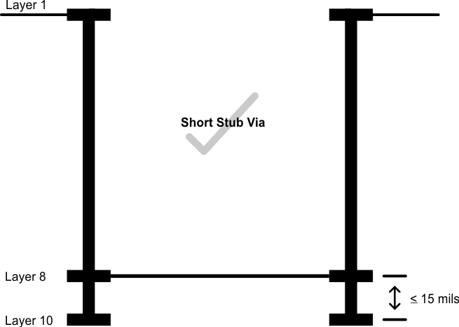
Because longer via stubs resonate at lower frequencies and increase insertion loss, keep these stubs as short as possible. In most cases, the stub portion of the via present significantly more signal degradation than the signal portion of the via. TI recommends keeping via stubs to less than 15 mils. Longer stubs must be back-drilled.
For examples of short and long via lengths, see #SPRAAR73400 and #SPRAAR7209.
 Figure 3-5 Via
Length (Long Stub)
 Figure 3-6 Via
Length (Short Stub)