SPRAAR7J November 2018 – February 2023 66AK2G12 , AM1806 , AM1808 , AM2431 , AM2432 , AM2434 , AM3351 , AM3352 , AM3354 , AM3356 , AM3357 , AM3358 , AM3358-EP , AM3359 , AM3871 , AM3874 , AM3892 , AM3894 , AM4376 , AM4377 , AM4378 , AM4379 , AM5706 , AM5708 , AM5716 , AM5718 , AM5726 , AM5728 , AM5729 , AM5746 , AM5748 , AM5749 , AM620-Q1 , AM623 , AM625 , AM625-Q1 , AM625SIP , AM62A1-Q1 , AM62A3 , AM62A3-Q1 , AM62A7 , AM62A7-Q1 , AM62P , AM62P-Q1 , AM6411 , AM6412 , AM6421 , AM6422 , AM6441 , AM6442 , AM6526 , AM6528 , AM6546 , AM6548 , BQ24392-Q1 , HD3SS6126 , LP8727 , OMAP-L137 , OMAP5912 , TMS320C6745 , TMS320DM355 , TMS320DM365 , TMS320DM368 , TMS320DM369 , TMS320DM6441 , TMS320DM6443 , TMS320DM6446 , TMS320DM6467 , TMS320DM8127 , TMS320DM8147 , TMS320DM8148 , TMS320DM8165 , TMS320DM8167 , TMS320DM8168 , TMS320VC5506 , TMS320VC5507 , TMS320VC5509A , TS3USB221A-Q1 , TS3USBA225 , TSU5511 , TSU5611 , TSU6111 , TSU6111A , TSU6721 , TSU8111
- Abstract
- Trademarks
- 1Introduction
- 2General High-Speed Signal Routing
-
3High-Speed Differential Signal Routing
- 3.1 Differential Signal Spacing
- 3.2 High-Speed Differential Signal Rules
- 3.3 Symmetry in the Differential Pairs
- 3.4 Crosstalk Between the Differential Signal Pairs
- 3.5 Connectors and Receptacles
- 3.6 Via Discontinuity Mitigation
- 3.7 Back-Drill Stubs
- 3.8 Increase Via Anti-Pad Diameter
- 3.9 Equalize Via Count
- 3.10 Surface-Mount Device Pad Discontinuity Mitigation
- 3.11 Signal Bending
- 3.12 Suggested PCB Stackups
- 3.13 ESD/EMI Considerations
- 3.14 ESD/EMI Layout Rules
- 4References
- A Device Layout Parameters
- Revision History
2.4 High-Speed Signal Reference Planes
High-speed signals should be routed over a solid GND reference plane and not across a plane split or a void in the reference plane unless absolutely necessary. TI does not recommend high-speed signal references to power planes.
Routing across a plane split or a void in the reference plane forces return high-frequency current to flow around the split or void. This can result in the following conditions:
- Excess radiated emissions from an unbalanced current flow
- Delays in signal propagation delays due to increased series inductance
- Interference with adjacent signals
- Degraded signal integrity (that is, more jitter and reduced signal amplitude)
For examples of correct and incorrect plane void routing, see #SPRAAR7919 and #SPRAAR75896.
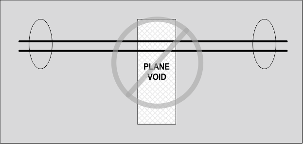 Figure 2-6 Incorrect
Plane Void Routing
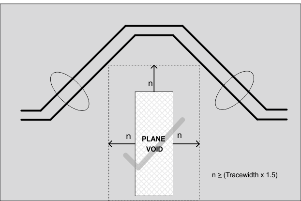 Figure 2-7 Correct
Plane Void Routing
Figure 2-7 Correct
Plane Void RoutingIf routing over a plane-split is completely unavoidable, place stitching capacitors across the split to provide a return path for the high-frequency current. These stitching capacitors minimize the current loop area and any impedance discontinuity created by crossing the split. These capacitors should be 1 µF or lower and placed as close as possible to the plane crossing. For examples of incorrect plane-split routing and correct stitch capacitor placement, see #SPRAAR76296 and #SPRAAR79964.
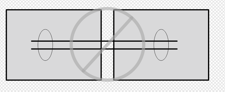 Figure 2-8 Incorrect
Plane-Split Signal Routing
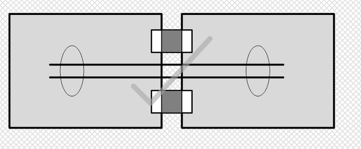 Figure 2-9 Stitching
Capacitor Placement
Figure 2-9 Stitching
Capacitor PlacementWhen planning a PCB stackup, ensure that planes that do not reference each other are not overlapped because this produces unwanted capacitance between the overlapping areas. To see an example of how this capacitance could pass RF emissions from one plane to the other, see #SPRAAR71342.
 Figure 2-10 Overlapped Planes
The entirety of any high-speed signal trace should maintain the same GND reference from origination to termination. If unable to maintain the same GND reference, via-stitch both GND planes together to ensure continuous grounding and uniform impedance. Place these stitching vias symmetrically within 200 mils (center-to-center, closer is better) of the signal transition vias. For an example of stitching vias, see #SPRAAR7481.
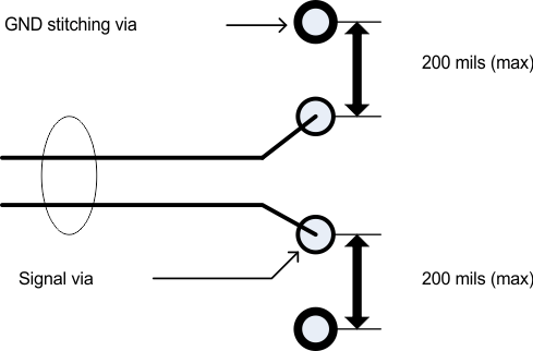 Figure 2-11 Stitching
Vias