SPRSPA1B March   2025  – November 2025 AM62L

PRODUCTION DATA  

  1.   1
  2. Features
  3. Applications
  4. Description
    1. 3.1 Functional Block Diagram
  5. Device Comparison
    1. 4.1 Related Products
  6. Terminal Configuration and Functions
    1. 5.1 Pin Diagrams
    2. 5.2 Pin Attributes
      1.      11
      2.      12
    3. 5.3 Signal Descriptions
      1.      14
      2. 5.3.1  ADC
        1. 5.3.1.1 MAIN Domain
          1.        17
      3. 5.3.2  CPSW3G
        1. 5.3.2.1 MAIN Domain
          1.        20
          2.        21
          3.        22
          4.        23
      4. 5.3.3  CPTS
        1. 5.3.3.1 MAIN Domain
          1.        26
      5. 5.3.4  DDRSS
        1. 5.3.4.1 MAIN Domain
          1.        29
      6. 5.3.5  DSI
        1. 5.3.5.1 MAIN Domain
          1.        32
      7. 5.3.6  DSS
        1. 5.3.6.1 MAIN Domain
          1.        35
      8. 5.3.7  ECAP
        1. 5.3.7.1 MAIN Domain
          1.        38
          2.        39
          3.        40
      9. 5.3.8  Emulation and Debug
        1. 5.3.8.1 MAIN Domain
          1.        43
        2. 5.3.8.2 WKUP Domain
          1.        45
      10. 5.3.9  EPWM
        1. 5.3.9.1 MAIN Domain
          1.        48
          2.        49
          3.        50
          4.        51
      11. 5.3.10 EQEP
        1. 5.3.10.1 MAIN Domain
          1.        54
          2.        55
          3.        56
      12. 5.3.11 GPIO
        1. 5.3.11.1 MAIN Domain
          1.        59
        2. 5.3.11.2 WKUP Domain
          1.        61
      13. 5.3.12 GPMC
        1. 5.3.12.1 MAIN Domain
          1.        64
      14. 5.3.13 I2C
        1. 5.3.13.1 MAIN Domain
          1.        67
          2.        68
          3.        69
          4.        70
        2. 5.3.13.2 WKUP Domain
          1.        72
      15. 5.3.14 MCAN
        1. 5.3.14.1 MAIN Domain
          1.        75
          2.        76
          3.        77
      16. 5.3.15 MCASP
        1. 5.3.15.1 MAIN Domain
          1.        80
          2.        81
          3.        82
      17. 5.3.16 MCSPI
        1. 5.3.16.1 MAIN Domain
          1.        85
          2.        86
          3.        87
          4.        88
      18. 5.3.17 MDIO
        1. 5.3.17.1 MAIN Domain
          1.        91
      19. 5.3.18 MMC
        1. 5.3.18.1 MAIN Domain
          1.        94
          2.        95
          3.        96
      20. 5.3.19 OSPI
        1. 5.3.19.1 MAIN Domain
          1.        99
      21. 5.3.20 Power Supply
        1.       101
      22. 5.3.21 Reserved
        1.       103
      23. 5.3.22 System and Miscellaneous
        1. 5.3.22.1 Boot Mode Configuration
          1. 5.3.22.1.1 MAIN Domain
            1.         107
        2. 5.3.22.2 Clock
          1. 5.3.22.2.1 RTC Domain
            1.         110
          2. 5.3.22.2.2 WKUP Domain
            1.         112
        3. 5.3.22.3 System
          1. 5.3.22.3.1 MAIN Domain
            1.         115
          2. 5.3.22.3.2 RTC Domain
            1.         117
          3. 5.3.22.3.3 WKUP Domain
            1.         119
      24. 5.3.23 TIMER
        1. 5.3.23.1 MAIN Domain
          1.        122
        2. 5.3.23.2 WKUP Domain
          1.        124
      25. 5.3.24 UART
        1. 5.3.24.1 MAIN Domain
          1.        127
          2.        128
          3.        129
          4.        130
          5.        131
          6.        132
          7.        133
        2. 5.3.24.2 WKUP Domain
          1.        135
      26. 5.3.25 USB
        1. 5.3.25.1 MAIN Domain
          1.        138
          2.        139
    4. 5.4 Pin Connectivity Requirements
  7. Specifications
    1. 6.1  Absolute Maximum Ratings
    2. 6.2  ESD Ratings
    3. 6.3  Power-On Hours (POH)
    4. 6.4  Recommended Operating Conditions
    5. 6.5  Operating Performance Points
    6. 6.6  Power Consumption Summary
    7. 6.7  Electrical Characteristics
      1. 6.7.1  I2C Open-Drain, and Fail-Safe (I2C OD FS) Electrical Characteristics
      2. 6.7.2  Fail-Safe Reset (FS RESET) Electrical Characteristics
      3. 6.7.3  High-Frequency Oscillator (HFOSC) Electrical Characteristics
      4. 6.7.4  Low-Frequency Oscillator (LFXOSC) Electrical Characteristics
      5. 6.7.5  SDIO Electrical Characteristics
      6. 6.7.6  LVCMOS Electrical Characteristics
      7. 6.7.7  1P8-LVCMOS Electrical Characteristics
      8. 6.7.8  RTC-LVCMOS Electrical Characteristics
      9. 6.7.9  ADC Electrical Characteristics
      10. 6.7.10 DSI (D-PHY) Electrical Characteristics
      11. 6.7.11 USB2PHY Electrical Characteristics
      12. 6.7.12 DDR Electrical Characteristics
    8. 6.8  VPP Specifications for One-Time Programmable (OTP) eFuses
      1. 6.8.1 Recommended Operating Conditions for OTP eFuse Programming
      2. 6.8.2 Hardware Requirements
      3. 6.8.3 Programming Sequence
      4. 6.8.4 Impact to Your Hardware Warranty
    9. 6.9  Thermal Resistance Characteristics
      1. 6.9.1 Thermal Resistance Characteristics for ANB Package
    10. 6.10 Temperature Sensor Characteristics
    11. 6.11 Timing and Switching Characteristics
      1. 6.11.1 Timing Parameters and Information
      2. 6.11.2 Power Supply Requirements
        1. 6.11.2.1 Power Supply Slew Rate Requirement
        2. 6.11.2.2 Power Supply Sequencing
          1. 6.11.2.2.1 No Low-Power Mode Sequencing
          2. 6.11.2.2.2 RTC Only Low-Power Mode Sequencing
          3. 6.11.2.2.3 RTC + IO + DDR Low-Power Mode Sequencing
      3. 6.11.3 System Timing
        1. 6.11.3.1 Reset Timing
        2. 6.11.3.2 Clock Timing
      4. 6.11.4 Clock Specifications
        1. 6.11.4.1 Input Clocks / Oscillators
          1. 6.11.4.1.1 WKUP_OSC0 Internal Oscillator Clock Source
            1. 6.11.4.1.1.1 Load Capacitance
            2. 6.11.4.1.1.2 Shunt Capacitance
          2. 6.11.4.1.2 WKUP_OSC0 LVCMOS Digital Clock Source
          3. 6.11.4.1.3 LFOSC0 Internal Oscillator Clock Source
          4. 6.11.4.1.4 LFOSC0 LVCMOS Digital Clock Source
          5. 6.11.4.1.5 LFOSC0 Not Used
        2. 6.11.4.2 Output Clocks
        3. 6.11.4.3 PLLs
        4. 6.11.4.4 Recommended System Precautions for Clock and Control Signal Transitions
      5. 6.11.5 Peripherals
        1. 6.11.5.1  CPSW3G
          1. 6.11.5.1.1 CPSW3G MDIO Timing
          2. 6.11.5.1.2 CPSW3G RMII Timing
          3. 6.11.5.1.3 CPSW3G RGMII Timing
        2. 6.11.5.2  CPTS
        3. 6.11.5.3  DDRSS
        4. 6.11.5.4  DSI
        5. 6.11.5.5  DSS
        6. 6.11.5.6  ECAP
        7. 6.11.5.7  Emulation and Debug
          1. 6.11.5.7.1 Trace
          2. 6.11.5.7.2 JTAG
        8. 6.11.5.8  EPWM
        9. 6.11.5.9  EQEP
        10. 6.11.5.10 GPIO
        11. 6.11.5.11 GPMC
          1. 6.11.5.11.1 GPMC and NOR Flash — Synchronous Mode
          2. 6.11.5.11.2 GPMC and NOR Flash — Asynchronous Mode
          3. 6.11.5.11.3 GPMC and NAND Flash — Asynchronous Mode
        12. 6.11.5.12 I2C
        13. 6.11.5.13 MCAN
        14. 6.11.5.14 MCASP
        15. 6.11.5.15 MCSPI
          1. 6.11.5.15.1 MCSPI — Controller Mode
          2. 6.11.5.15.2 MCSPI — Peripheral Mode
        16. 6.11.5.16 MMCSD
          1. 6.11.5.16.1 MMC0 - eMMC/SD/SDIO Interface
            1. 6.11.5.16.1.1  Legacy SDR Mode
            2. 6.11.5.16.1.2  High Speed SDR Mode
            3. 6.11.5.16.1.3  High Speed DDR Mode
            4. 6.11.5.16.1.4  HS200 Mode
            5. 6.11.5.16.1.5  Default Speed Mode
            6. 6.11.5.16.1.6  High Speed Mode
            7. 6.11.5.16.1.7  UHS–I SDR12 Mode
            8. 6.11.5.16.1.8  UHS–I SDR25 Mode
            9. 6.11.5.16.1.9  UHS–I SDR50 Mode
            10. 6.11.5.16.1.10 UHS–I DDR50 Mode
            11. 6.11.5.16.1.11 UHS–I SDR104 Mode
          2. 6.11.5.16.2 MMC1/MMC2 - SD/SDIO Interface
            1. 6.11.5.16.2.1 Default Speed Mode
            2. 6.11.5.16.2.2 High Speed Mode
            3. 6.11.5.16.2.3 UHS–I SDR12 Mode
            4. 6.11.5.16.2.4 UHS–I SDR25 Mode
            5. 6.11.5.16.2.5 UHS–I SDR50 Mode
            6. 6.11.5.16.2.6 UHS–I DDR50 Mode
            7. 6.11.5.16.2.7 UHS–I SDR104 Mode
        17. 6.11.5.17 OSPI
          1. 6.11.5.17.1 OSPI0 PHY Mode
            1. 6.11.5.17.1.1 OSPI0 With PHY Data Training
            2. 6.11.5.17.1.2 OSPI0 Without Data Training
              1. 6.11.5.17.1.2.1 OSPI0 PHY SDR Timing
          2. 6.11.5.17.2 OSPI0 Tap Mode
            1. 6.11.5.17.2.1 OSPI0 Tap SDR Timing
            2. 6.11.5.17.2.2 OSPI0 Tap DDR Timing
        18. 6.11.5.18 Timers
        19. 6.11.5.19 UART
        20. 6.11.5.20 USB
  8. Detailed Description
    1. 7.1 Overview
    2. 7.2 Processor Subsystem
      1. 7.2.1 Arm Cortex-A53 Subsystem (A53SS)
    3. 7.3 Other Subsystem
      1. 7.3.1 Data Movement Subsystem (DMSS)
      2. 7.3.2 Peripheral DMA Controller (PDMA)
    4. 7.4 Peripherals
      1. 7.4.1  ADC
      2. 7.4.2  Gigabit Ethernet Switch (CPSW3G)
      3. 7.4.3  DDR Subsystem (DDRSS)
      4. 7.4.4  Display Subsystem (DSS)
      5. 7.4.5  Enhanced Capture (ECAP)
      6. 7.4.6  Error Location Module (ELM)
      7. 7.4.7  Enhanced Pulse Width Modulation (EPWM)
      8. 7.4.8  Enhanced Quadrature Encoder Pulse (EQEP)
      9. 7.4.9  General-Purpose Interface (GPIO)
      10. 7.4.10 General-Purpose Memory Controller (GPMC)
      11. 7.4.11 Global Timebase Counter (GTC)
      12. 7.4.12 Inter-Integrated Circuit (I2C)
      13. 7.4.13 Modular Controller Area Network (MCAN)
      14. 7.4.14 Multichannel Audio Serial Port (MCASP)
      15. 7.4.15 Multichannel Serial Peripheral Interface (MCSPI)
      16. 7.4.16 Multi-Media Card Secure Digital (MMCSD)
      17. 7.4.17 Octal Serial Peripheral Interface (OSPI)
      18. 7.4.18 Timers
      19. 7.4.19 Real-Time Clock (RTC)
      20. 7.4.20 Universal Asynchronous Receiver/Transmitter (UART)
      21. 7.4.21 Universal Serial Bus Subsystem (USBSS)
  9. Applications, Implementation, and Layout
    1. 8.1 Device Connection and Layout Fundamentals
      1. 8.1.1 Power Supply
        1. 8.1.1.1 Power Supply Designs
        2. 8.1.1.2 Power Distribution Network Implementation Guidance
      2. 8.1.2 External Oscillator
      3. 8.1.3 JTAG, EMU, and TRACE
      4. 8.1.4 Unused Pins
    2. 8.2 Peripheral- and Interface-Specific Design Information
      1. 8.2.1 DDR Board Design and Layout Guidelines
      2. 8.2.2 OSPI/QSPI/SPI Board Design and Layout Guidelines
        1. 8.2.2.1 No Loopback, Internal PHY Loopback, and Internal Pad Loopback
        2. 8.2.2.2 External Board Loopback
        3. 8.2.2.3 DQS (only available in Octal SPI devices)
      3. 8.2.3 USB VBUS Design Guidelines
      4. 8.2.4 High Speed Differential Signal Routing Guidance
      5. 8.2.5 Thermal Solution Guidance
    3. 8.3 Clock Routing Guidelines
      1. 8.3.1 Oscillator Routing
  10. Device and Documentation Support
    1. 9.1 Device Nomenclature
      1. 9.1.1 Standard Package Symbolization
      2. 9.1.2 Device Naming Convention
    2. 9.2 Tools and Software
    3. 9.3 Documentation Support
    4. 9.4 Support Resources
    5. 9.5 Trademarks
    6. 9.6 Electrostatic Discharge Caution
    7. 9.7 Glossary
  11.   Revision History
  12. 10Mechanical, Packaging, and Orderable Information
    1. 10.1 Packaging Information

Package Options

Refer to the PDF data sheet for device specific package drawings

Mechanical Data (Package|Pins)
  • ANB|373
Thermal pad, mechanical data (Package|Pins)
Orderable Information

USB VBUS Design Guidelines

The USB 3.1 specification allows the VBUS voltage to be as high as 5.5V for normal operation, and as high as 20V when the Power Delivery addendum is supported. Some automotive applications require a max voltage to be 30V.

The device requires the VBUS signal voltage be scaled down using an external resistor divider (as shown in the Figure 8-4), which limits the voltage applied to the actual device pin (USB0_VBUS). The tolerance of these external resistors should be equal to or less than 1%, and the leakage current of Zener diode at 5V should be less than 100nA.
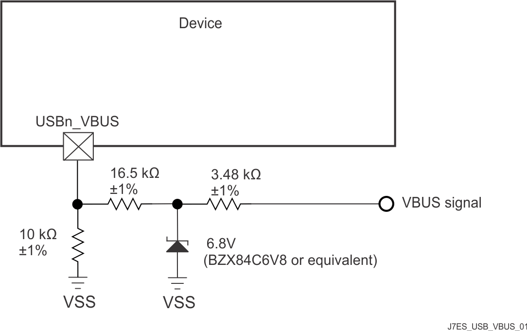
AM62L USB VBUS Detect Voltage Divider /
          Clamp Circuit Figure 8-4 USB VBUS Detect Voltage Divider / Clamp Circuit

The USB0_VBUS pin can be considered to be fail-safe because the external circuit in Figure 8-4 limits the input current to the actual device pin in a case where VBUS is applied while the device is powered off.