SLYY234 December 2024 AMC0106M05 , AMC0106M25 , AMC0136 , AMC0311D , AMC0311S , AMC0386 , AMC0386-Q1 , AMC1100 , AMC1106M05 , AMC1200 , AMC1200-Q1 , AMC1202 , AMC1203 , AMC1204 , AMC1211-Q1 , AMC1300 , AMC1300B-Q1 , AMC1301 , AMC1301-Q1 , AMC1302-Q1 , AMC1303M2510 , AMC1304L25 , AMC1304M25 , AMC1305M25 , AMC1305M25-Q1 , AMC1306M05 , AMC1306M25 , AMC1311 , AMC1311-Q1 , AMC131M03 , AMC1336 , AMC1336-Q1 , AMC1350 , AMC1350-Q1 , AMC23C12 , AMC3301 , AMC3330 , AMC3330-Q1
- 1
- Introduction
- Introduction to Isolated Signal Chain
- Selection Trees
-
Current Sensing
- Shunt Resistor Selection for Isolated Data Converters
- Design considerations for isolated current sensing
- Isolated Current-Sensing Circuit With ±50-mV Input and Single-Ended Output
- Isolated Current-Sensing Circuit With ±50-mV Input and Differential Output
- Isolated Current-Sensing Circuit With ±250-mV Input Range and Single-Ended Output Voltage
- Isolated current-measurement circuit with ±250-mV input and differential output
- Isolated Overcurrent Protection Circuit
- Interfacing a Differential-Output (Isolated) Amp to a Single-Ended Input ADC
- Utilizing AMC3311 to Power AMC23C11 for Isolated Sensing and Fault Detection
- Isolated Current-Sensing Circuit With Front-End Gain Stage
- Accuracy Comparison of Isolated Shunt and Closed-Loop Current Sensing
-
Voltage Sensing
- Maximizing Power Conversion and Motor Control Efficiency With Isolated Voltage Sensing
- Increased Accuracy and Performance with Integrated High Voltage Resistor Isolated Amplifiers and Modulators
- Isolated Amplifiers With Differential, Single-Ended Fixed Gain and Ratiometric Outputs for Voltage Sensing Applications
- Isolated Voltage-Measurement Circuit With ±250-mV Input and Differential Output
- Split-Tap Connection for Line-to-Line Isolated Voltage Measurement Using AMC3330
- ±12V Voltage Sensing Circuit With an Isolated Amplifier and Pseudo-Differential Input SAR ADC
- ±12-V voltage sensing circuit with an isolated amplifier and differential input SAR ADC
- Isolated Undervoltage and Overvoltage Detection Circuit
- Isolated Zero-Cross Detection Circuit
- ±480V Isolated Voltage-Sensing Circuit With Differential Output
-
EMI Performance
- Best in Class Radiated Emissions EMI Performance with Isolated Amplifiers
- Best Practices to Attenuate AMC3301 Family Radiated Emissions EMI
-
End Equipment
- Comparing Shunt- and Hall-Based Isolated Current-Sensing Solutions in HEV/EV
-
Design Considerations for Current Sensing
in DC EV Charging Applications
- Abstract
- Introduction
-
Current Sensing in AC/DC Converters
- Basic Hardware and Control Description of AC/DC
- Point A and B – AC/DC AC Phase-Current Sensing
- Point C and D – AC/DC DC Link Current Sensing
- Summary of Positives and Negatives at Point A, B, C1/2 and D1/2 and Product Suggestions
- Current Sensing in DC/DC Converters
- Conclusion
- References
-
Using isolated comparators for fault
detection in electric motor drives
- Introduction
- Introduction to electric motor drives
- Understanding fault events in electric motor drives
- Achieving reliable detection and protection in electric motor drives
- Use case No. 1: Bidirectional in-phase overcurrent detection
- Use case No. 2: DC+ overcurrent detection
- Use case No. 3: DC– overcurrent or short-circuit detection
- Use case No. 4: DC-link (DC+ to DC–) overvoltage and undervoltage detection
- Use case No. 5: IGBT module overtemperature detection
- Discrete DESAT for Opto-Compatible Isolated Gate Driver UCC23513 in Motor Drives
- Isolated voltage sensing in AC motor drives
- Achieving High-Performance Isolated Current and Voltage Sensing in Server PSUs
-
Additional Reference Designs/Circuits
- Designing a Bootstrap Charge-Pump Power Supply for an Isolated Amplifier
-
Clock Edge Delay Compensation With
Isolated Modulators Digital Interface to MCUs
- Abstract
- Introduction
- Design Challenge With Digital Interface Timing Specifications
- Design Approach With Clock Edge Delay Compensation
- Test and Validation
- Conclusion
- References
- Utilizing AMC3311 to Power AMC23C11 for Isolated Sensing and Fault Detection
Design Goals
| Voltage Source | AMC1300B Input Voltage | AMC1300B Output Voltage (1.44VCM) | Power Supplies | ||||
|---|---|---|---|---|---|---|---|
| VMAX | VMIN | VIN DIFF, MAX | VIN DIFF, MIN | VOUT DIFF, MAX | VOUT DIFF, MIN | VDD1 | VDD2 |
| +240V | –240V | +250mV | –250mV | +2.05V | –2.05V | 3.0V–5.5V | 3.0V–5.5V |
Design Description I
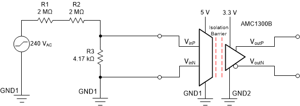
This circuit performs a high-voltage, differential measurement using a voltage divider and a ±250-mV differential input, differential output, AMC1300B isolated amplifier. Because it is a low-input impedance device, the AMC1300B is better suited for current sensing applications. The interaction of the input impedance of the isolated amplifier and the input voltage divider introduces a gain error. Additionally, bias current passing out of the low-impedance inputs and through the voltage sense resistor causes a significant offset error. We will first design without compensating for these errors. Then, we will observe their effects and describe them mathematically. Finally, we will redesign to limit their effects and observe the improved results.
The voltage-divider circuit reduces the input voltage from ±240V to ±250mV so as to match the input range of the isolation amplifier. The AMC1300B requires both high- and low-side power supplies. The high-side supply will often be generated using a floating supply or from the low side using an isolated transformer or isolated DC/DC converter. The AMC1300B can measure differential signals of ±250mV with a fixed gain of 8.2V/V and output an isolated differential output voltage of ±2.05V with an output common-mode voltage of 1.44V. The differential output voltage can be scaled as necessary using an additional operational amplifier, as shown in Interfacing a Differential-Output (Isolated) Amplifier to a Single-Ended Input ADC Tech Note with the TLV6001 device, to interface with an ADC.
Design Notes I
- Verify that the isolation amplifier will remain in its linear region of operation for the desired input signal range. This can be achieved using a DC sweep simulation as demonstrated in the DC Transfer Characteristics I section.
- Ensure the resistors used in the resistor divider circuit (R1–R3) are capable of dissipating the power supplied from the voltage source.
- Check that the input voltage applied to the device will remain within the range specified by the data sheet. Should the input range be violated, ensure that the input current remains below 10 mA to avoid damaging the part. If the system is susceptible to transient events, consider adding TVS diodes to the inputs.
Design Steps I
- Calculate the required voltage
divider attenuation based on the ratio of the input voltage source
(Vsource) to the full-scale input voltage of the AMC1300B (VIN_AMC_FSR).
- Select a resistance for the top
portion of the voltage divider (R1 and R2). Note that power consumption is equal
to I2R and by Ohm's law, current and resistivity are inversely
proportional. A linear increase in resistivity will lead to a linear decrease in
power. For this reason, choosing large resistance values will minimize overall
power consumption. These components dominate the power consumption of the
voltage divider. So, select the value of Rtop to meet a peak power specification
for the voltage divider.
- Split the Rtop resistance value
into multiple resistors to minimize the power rating required of each resistor.
- Next, assume
the input resistance of the isolation amplifier is large. The input voltage seen
by the part from the voltage source will be determined by the voltage divider
effect created by Rtop with R3. Solve for R3.
DC Transfer Characteristics I
The following graphs show the simulated output for a ±240V source. The source is swept from –300V to +300V and the input and output voltages of the amplifier are observed. The desired linear ranges are ±250mV at the input of the amplifier and ±2.05V at the output of the amplifier. At the input of the amplifier, we expect to see an offset error of 0 and a gain of about 1.042mV/V due to the voltage division of the voltage divider. At the output of the amplifier, we again expect to see an offset error of 0 and a gain of 8.542mV/V due to the attenuation of the voltage source of the voltage divider followed by the fixed 8.2V/V gain of the AMC1300B.
As can be seen in the following graphs , the simulated results do not match the desired, ideal output. At the input of the amplifier, an offset voltage error of 107mV is present. This is significant when compared to the ±250-mV input range of the part. This offset error is carried over to the output of the amplifier, where an 837-mV offset takes up a large portion of the ±2.05-V output range of the amplifier. The circuit also demonstrates a significant gain error. Despite expecting a gain of 1.042mV/V at the input from the voltage divider and 8.540mV/V at the output of the device, we instead observe gains of 0.853mV/V and 6.842mV/V, respectively, yielding large gain errors of approximately 18.1% and 19.9%. The following section will define better design practices.


Design Description II
The previous method is appropriate for voltage sensing applications when using devices with large input resistances, such as 1MΩ or greater. The AMC1300B device has a differential input impedance of 22kΩ which leads to the offset and gain errors shown previously. Gain and offset errors when using a low-input impedance amp for voltage sensing in this circuit configuration can be estimated using the following formulas.
The gain error is a result of a non-ideal voltage division by R3. Because the input resistance of the amplifier is comparable in size to R3, some of the current passing out of R1 and R2 will not pass through R3, but instead pass through the input of the amplifier. The result will be an unexpected voltage drop at the input of the amplifier. Consequently, the formula presented in 4 of the Design Steps I section will not be valid and a more complete formula that considers the input impedance of the amplifier being parallel to R3 must be considered. The offset error is the product of the bias current flowing out of the positive input pin of the isolated amplifier, through the shunt resistor, R3. This bias current across R3 can lead to significant offset voltages at the input that are then amplified and passed to the output.
Using the previous formulas allows one to estimate the errors of the circuit in the Design Steps I section. Using the typical data sheet values, the differential input resistance is 22kΩ and the input bias current is 30µA. Our designed value for R3 is 4.17kΩ and as a result one would expect to see a gain error of 18.7% and an offset error of 125mV at the input of the amplifier. In comparison, the simulated errors had a gain error of 19.9% at the output of the amplifier and 107mV of offset at the input. These error formulas serve as valuable tools to get a quick idea of the expected magnitude of the errors. Without needing to perform simulations, one can get an idea of whether or not the expected errors will be acceptable for the end use case.
As noted in the AMC1300 Precision, ±250-mV Input, Reinforced Isolated Amplifier Data Sheet, for voltage sensing applications the introduction of R3' in series with the inverting terminal of the amplifier can reduce the offset and gain errors. The bias current of the amplifier will generate a similar offset at the negative input pin as at the positive input pin. This will greatly reduce the magnitude of the overall offset voltage. Additionally, the effects of the input resistance of the amplifier and R3' will be taken into account when selecting the value of R3. This will provide a more ideal voltage division of the 240-V source and will improve the overall gain error.
Design Steps II - Consideration of R3'
As in Design Steps I, the Gain and Rtop resistance calculations are exactly the same, we are more interested in calculating R3 and R3' to provide the best circuit performance.
- Note that the bottom portion of the
resistor divider will set the input voltage range for the isolation amplifier.
The ideal value for R3 is dependent on the gain, Rtop and Rind, where Rind is
the differential input impedance of the amplifier. As a reminder, Rtop is the
combination of R1 + R2.
- The purpose of R3’ is to cancel out
the gain error introduced by the bias current flowing through R3. The ideal R3’
would be the parallel combination of Rtop and R3. Use the following equation to
calculate R3’.
This is the resulting ideal circuit configuration. Note that Rind, shown in red, is shown to represent the differential input resistance of the AMC1300B and should not be added to the schematic.

DC Transfer Characteristics II
The following graphs show the simulated output for a ±240-V source using the new design. Recall that the desired linear ranges are ±250mV at the input of the amplifier and ±2.05V at the output of the amplifier.


Clearly, the new design offers a dramatically improved offset error. The input offset voltage and gain error have been reduced to zero. The revised circuit also demonstrates better gain error performance due to the more accurate calculation used to find the desired value of R3 for the input voltage divider and the ideal value for R3’.
This positive outcome is a consequence of the addition of R3’ to cancel the offset voltage introduced in the original design by the bias current of the AMC1300B device through R3. The drawback is that the ideal values for R3 and R3’ are not commercially available, and in reality it would not be practical to use two different resistor values which are so close together.
Using the Analog Engineers Calculator, it is possible to find the nearest E189 series resistor values that are readily available. In both cases, the nearest 0.1% resistor value to the calculated ideal values for R3 and R3’ are 6.65kΩ. The final circuit diagram follows.

With readily available resistors used for R3 and R3', the circuit performance is still quite good as can be seen in the following graphs. The gain error on the input has been reduced from 18.2% to 0.3%. The gain error at the output has been reduced from 19.9% to 0.4%. The offset errors are also reduced to 195µV on the input and 2mV at the output.


AC Transfer Characteristics II
An AC sweep validates the frequency range across which one can expect to see the desired output. From the following simulation plot, the simulated gain of –41.40 dB, or 8.51mV/V, matches the gain result from the DC output plot. This is relatively close to the desired output gain of –41.37dB, or 8.54mV/V, as discussed in the previous section. The simulated bandwidth of the design, 313.1kHz, slightly exceeds the expectation set by the typical bandwidth specification of 310kHz in the data sheet.

References
Design Featured Isolated Op Amp
| AMC1300B | |
|---|---|
| VDD1 | 3.0V–5.5V |
| VDD2 | 3V–5.5V |
| Input Voltage range | ±250mV |
| Nominal Gain | 8.2 |
| VOUT | Differential ±2.05V on output common-mode of 1.44V |
| Input Resistance | 19kΩ (typ, single-ended), 22kΩ (typ, differential) |
| Small Signal Bandwidth | 310kHz |
| Input Offset Voltage and Drift | ±0.2mV (max), ±3µV/°C (max) |
| Gain Error and Drift | ±0.3% (max), ±15 ppm/°C (typ) |
| Nonlinearity and Drift | ±0.03% (max), ±1 ppm/°C (typ) |
| Isolation Transient Overvoltage | 7.071kVPEAK |
| Working Voltage | 1.5kVRMS, 2.121kVDC |
| Common-mode transient immunity, CMTI | 75 kV/µs (min), 140 kV/µs (typ) |
| AMC1300 | |
Design Alternate Isolated Op Amp
| AMC1200 | |
|---|---|
| VDD1 | 4.5V–5.5V |
| VDD2 | 2.7V–5.5V |
| Input Voltage range | ±250mV |
| Nominal Gain | 8 |
| VOUT | Differential ±2V, common-mode varies with supply range |
| Input Resistance | 28kΩ (typ, differential) |
| Small Signal Bandwidth | 100kHz |
| Input Offset Voltage and Drift | ±1.5mV (max), ±10µV/°C (max) |
| Gain Error and Drift | ±1% (max), ±56 ppm/°C (typ) |
| Nonlinearity and Drift | ±0.1% (max), ±2.4 ppm/°C (typ) |
| Isolation Transient Overvoltage | 4kVPEAK |
| Working Voltage | 1.2kVpeak |
| Common-mode transient immunity, CMTI | 10kV/µs (min), 15kV/µs (typ) |
| AMC1200 | |