SLYY234 December 2024 AMC0106M05 , AMC0106M25 , AMC0136 , AMC0311D , AMC0311S , AMC0386 , AMC0386-Q1 , AMC1100 , AMC1106M05 , AMC1200 , AMC1200-Q1 , AMC1202 , AMC1203 , AMC1204 , AMC1211-Q1 , AMC1300 , AMC1300B-Q1 , AMC1301 , AMC1301-Q1 , AMC1302-Q1 , AMC1303M2510 , AMC1304L25 , AMC1304M25 , AMC1305M25 , AMC1305M25-Q1 , AMC1306M05 , AMC1306M25 , AMC1311 , AMC1311-Q1 , AMC131M03 , AMC1336 , AMC1336-Q1 , AMC1350 , AMC1350-Q1 , AMC23C12 , AMC3301 , AMC3330 , AMC3330-Q1
- 1
- Introduction
- Introduction to Isolated Signal Chain
- Selection Trees
-
Current Sensing
- Shunt Resistor Selection for Isolated Data Converters
- Design considerations for isolated current sensing
- Isolated Current-Sensing Circuit With ±50-mV Input and Single-Ended Output
- Isolated Current-Sensing Circuit With ±50-mV Input and Differential Output
- Isolated Current-Sensing Circuit With ±250-mV Input Range and Single-Ended Output Voltage
- Isolated current-measurement circuit with ±250-mV input and differential output
- Isolated Overcurrent Protection Circuit
- Interfacing a Differential-Output (Isolated) Amp to a Single-Ended Input ADC
- Utilizing AMC3311 to Power AMC23C11 for Isolated Sensing and Fault Detection
- Isolated Current-Sensing Circuit With Front-End Gain Stage
- Accuracy Comparison of Isolated Shunt and Closed-Loop Current Sensing
-
Voltage Sensing
- Maximizing Power Conversion and Motor Control Efficiency With Isolated Voltage Sensing
- Increased Accuracy and Performance with Integrated High Voltage Resistor Isolated Amplifiers and Modulators
- Isolated Amplifiers With Differential, Single-Ended Fixed Gain and Ratiometric Outputs for Voltage Sensing Applications
- Isolated Voltage-Measurement Circuit With ±250-mV Input and Differential Output
- Split-Tap Connection for Line-to-Line Isolated Voltage Measurement Using AMC3330
- ±12V Voltage Sensing Circuit With an Isolated Amplifier and Pseudo-Differential Input SAR ADC
- ±12-V voltage sensing circuit with an isolated amplifier and differential input SAR ADC
- Isolated Undervoltage and Overvoltage Detection Circuit
- Isolated Zero-Cross Detection Circuit
- ±480V Isolated Voltage-Sensing Circuit With Differential Output
-
EMI Performance
- Best in Class Radiated Emissions EMI Performance with Isolated Amplifiers
- Best Practices to Attenuate AMC3301 Family Radiated Emissions EMI
-
End Equipment
- Comparing Shunt- and Hall-Based Isolated Current-Sensing Solutions in HEV/EV
-
Design Considerations for Current Sensing
in DC EV Charging Applications
- Abstract
- Introduction
-
Current Sensing in AC/DC Converters
- Basic Hardware and Control Description of AC/DC
- Point A and B – AC/DC AC Phase-Current Sensing
- Point C and D – AC/DC DC Link Current Sensing
- Summary of Positives and Negatives at Point A, B, C1/2 and D1/2 and Product Suggestions
- Current Sensing in DC/DC Converters
- Conclusion
- References
-
Using isolated comparators for fault
detection in electric motor drives
- Introduction
- Introduction to electric motor drives
- Understanding fault events in electric motor drives
- Achieving reliable detection and protection in electric motor drives
- Use case No. 1: Bidirectional in-phase overcurrent detection
- Use case No. 2: DC+ overcurrent detection
- Use case No. 3: DC– overcurrent or short-circuit detection
- Use case No. 4: DC-link (DC+ to DC–) overvoltage and undervoltage detection
- Use case No. 5: IGBT module overtemperature detection
- Discrete DESAT for Opto-Compatible Isolated Gate Driver UCC23513 in Motor Drives
- Isolated voltage sensing in AC motor drives
- Achieving High-Performance Isolated Current and Voltage Sensing in Server PSUs
-
Additional Reference Designs/Circuits
- Designing a Bootstrap Charge-Pump Power Supply for an Isolated Amplifier
-
Clock Edge Delay Compensation With
Isolated Modulators Digital Interface to MCUs
- Abstract
- Introduction
- Design Challenge With Digital Interface Timing Specifications
- Design Approach With Clock Edge Delay Compensation
- Test and Validation
- Conclusion
- References
- Utilizing AMC3311 to Power AMC23C11 for Isolated Sensing and Fault Detection
| ISO224 Input Voltage | ISO Output, ADC Input (VOUTP - VOUTN) | Digital Output ADS7945 |
|---|---|---|
| +12V | +4V | 1999H |
| –12V | –4V | E666H |
| Power Supplies and Reference Voltages | ||
|---|---|---|
| VDD1 | VDD2 and AVDD | REF5050 External Ref |
| 15V | 5V | 5V |
Design Description
This circuit performs a ±12-V isolated voltage sensing measurement utilizing the ISO224 isolated amplifier and the ADS745 SAR ADC. The ISO224 can measure true differential signals of ±12V with a fixed gain of ⅓V/V and produces an isolated differential output voltage with an output common-mode voltage of VDD2 / 2. The ADS7945 is a fully differential input ADC with a full-scale input voltage of ±VREF and a common-mode input voltage of VREF / 2 ±200mV. Selecting a +5-V reference allows the ADS7945 to accept the full-scale and common-mode outputs from the ISO224. Capturing the ISO224 output with a fully differential input ADC doubles the system dynamic range compared to a single-ended conversion. Many high-voltage industrial applications such as Protection Relays, Channel-to-Channel Isolated ±10V Analog Input Cards, and Inverter & Motor Control. The equations and explanation of component selection in this design can be customized based on system specifications and needs.

Specifications
| Specification | Calculated | Simulated |
|---|---|---|
| Transient ADC input settling at 100ksps | 305µV | 11µV |
| Conditioned signal range | ±4V | ±4V |
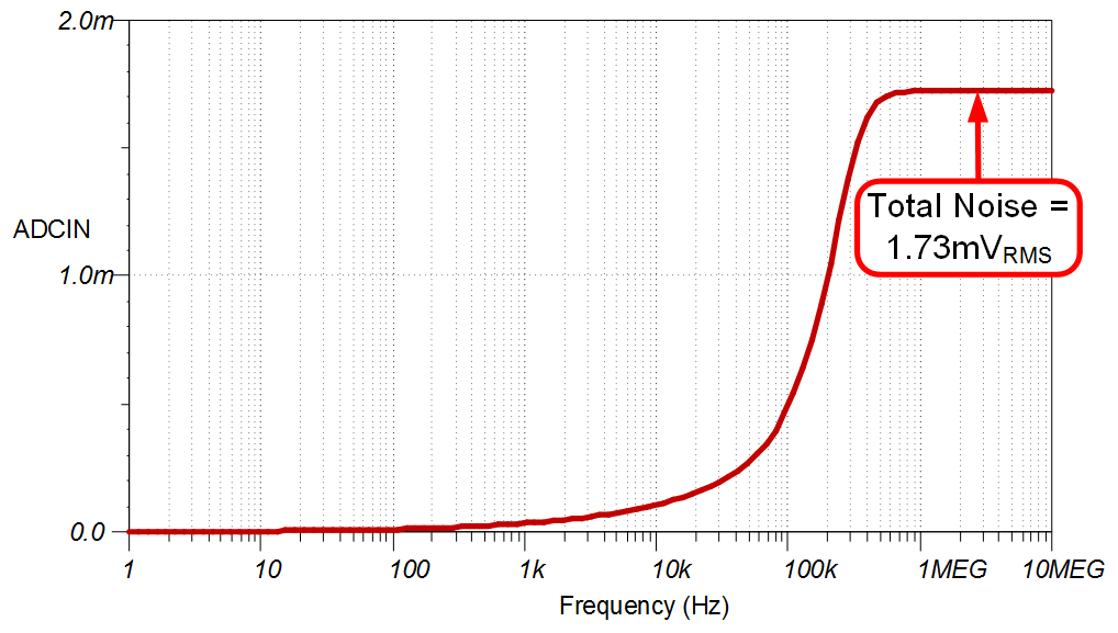
| Noise (at the input) | 1.9mVRMS | 1.73mVRMS |
| Closed-loop bandwidth | 175kHz | 185kHz |
Design Notes
- The ADS7945 was selected due to its low power and a compatible analog input structure with the ISO224.
- Verify the systems linear operation for the desired input signal range. This is verified using simulation in the DC Transfer Characteristics selection.
- Select COG capacitors for CFILT to minimize distortion.
- Understanding and Calibrating the Offset and Gain for ADC Systems covers methods for error analysis. Review the link for methods to minimize gain, offset, drift, and noise errors.
- The TI Precision Labs - ADCs training video series covers methods for selecting the charge bucket circuit RFILT and CFILT. These component values are dependent on the amplifier bandwidth, data converter sampling rate, and data converter design. The values shown here will give good settling and AC performance for the amplifier and data converter in this example. If the design is modified, a different RC filter must be selected. Refer to Introduction to SAR ADC Front-End Component Selection for an explanation of how to select the RC filter for best settling and AC performance.
Component Selection
- Select an isolated amplifier based
on the input voltage range and determine the output common-mode voltage and
output voltage range:
- ±12-V single-ended input range
- Fixed gain of ⅓, yielding ±4-V differential output
- Output common-mode voltage of +2.5V
- 4.5-V to 18-V high-side power supply, 4.5-V to 5.5-V low-side power supply
- Input Offset: ±5mV at 25°C, ±42µV/°C maximum
- Gain Error: ±0.3% at 25°C, ±50ppm/°C maximum
- Nonlinearity: ±0.01% max, ±1ppm/°C
- High-input impedance of 1.25MΩ
- Select an ADC with an appropriate
common-mode and differential input range to pair with the +2.5-V common-mode and
±4-V differential output of the ISO224:
- ±5-V maximum analog input range
- Full-scale input span set by ±voltage reference
- Input common-mode range of VREF / 2 ±0.2V
- 2.7-V to 5.25-V power supply
- High SNR of 84, low power of 11.6mW at 2Msps
- Select a voltage reference that
supports the common-mode constraint set by the 2.5-V common-mode output of the
ISO224 and the VREF / 2 ±0.2-V
common-mode input voltage of the ADS7945. This means that the reference output
voltage must be 5V, low noise, and a configurable input voltage is preferred:
- 5-V output
- 5.2-V to 18-V input voltage power supply
- 3μVPP/V noise
- Select R1FILT,
R2FILT, and CFILT for settling of the input signal and
sample rate of 100ksps:
Refine the RFILT and CFILT Values is a TI Precision Labs video showing the methodology for selecting RFILT and CFILT. The final value of 120Ω and 510pF proved to settle to well below ½ of a least significant bit (LSB) within the acquisition window.
DC Transfer Characteristics
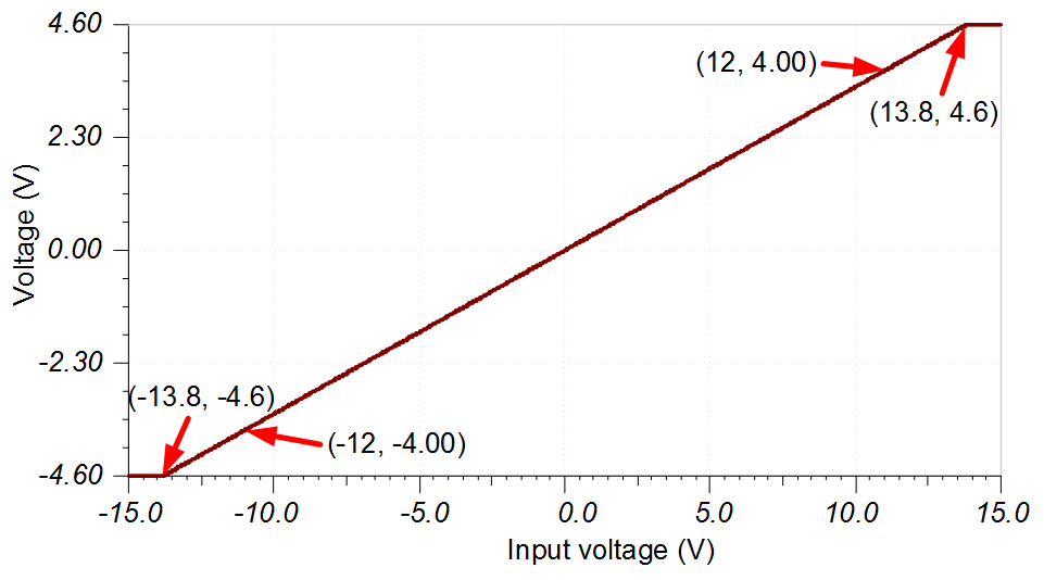
The following graph shows the simulated output for a ±15-V input. The desired linear range is a ±4-V output for a ±12-V input. This simulation shows that the linear output range is approximately ±4.6V which is well beyond the requirement.
The transfer function shows the ISO224 gain is ⅓ (that is, Gain · VIN = VOUT, (⅓)·(12V) = 4V).
AC Transfer Characteristics
The simulated bandwidth is approximately 186kHz and the gain is –9.57dB (or 0.332V/V) which closely matches the expected gain and bandwidth for the ISO224 (specified fc = 175kHz, gain = 0.333V/V).

Transient ADC Input Settling Simulation
The following simulation shows the transient settling results with an acquisition time of 9.6μs. The 11-μV settling error is well within the 0.5 × LSB limit of 305μV. See Refine the Rfilt and Cfilt Values for detailed theory on this subject.

Noise Simulation
The following noise calculation looks only at the noise of the ISO224. The ISO224 noise is substantially higher than other noise sources in the circuit, so the total noise can be approximated as the ISO224 noise. The same method can be used for the B grade.

The simulated noise is greater than the expected calculated noise. This difference is due to noise peaking in the simulation model. The noise peaking is not included in the calculation. Refer to Calculating the Total Noise for ADC Systems for detailed theory on this subject.
Design Featured Devices
| Device | Key Features | Link | Similar Devices |
|---|---|---|---|
| ISO224 | ±12-V single-ended input range, Fixed gain of ⅓, yielding ±4-V differential output, output common-mode voltage of +2.5V, 4.5-V to 18-V high-side power supply, 4.5-V to 5.5-V low side power supply, input offset: ±5mV at 25°C, ±42µV/°C max, gain error: ±0.3% at 25°C, ±50ppm/°C maximum, nonlinearity: ±0.01% maximum, ±1ppm/°C, high-input impedance of 1.25MΩ | www.ti.com/product/ISO224 | www.ti.com/isoamps |
| ADS7945 |
±5 V max analog input range, full-scale input span set by ±voltage reference, input common mode range of VREF / 2 ±0.2V, 2.7-V to 5.25-V power supply, high SNR of 84, low power of 11.6mW at 2Msps |
www.ti.com/product/ADS7945 | http://www.ti.com/opamps |
| REF5050 | 3ppm/°C drift, 0.05% initial accuracy, 4μVpp/V noise | www.ti.com/product/REF5050 | http://www.ti.com/vref |
Design References
See Analog Engineer's Circuit Cookbooks for TI's comprehensive circuit library.
Link to Key Files
See the TINA files for Isolated Design.