SZZA030E August 2021 – June 2022 CD4016B , CD4016B-MIL , CD4051B , CD4051B-MIL , CD4051B-Q1 , CD4052B , CD4052B-MIL , CD4053B , CD4053B-MIL , CD4053B-Q1 , CD4066B , CD4066B-MIL , CD4066B-Q1 , CD4067B , CD4067B-MIL , CD4097B , CD4097B-MIL , CD54HC4051 , CD54HC4052 , CD54HC4053 , CD54HC4066 , CD54HC4316 , CD54HC4351 , CD54HCT4051 , CD74HC4016 , CD74HC4051 , CD74HC4051-EP , CD74HC4051-Q1 , CD74HC4052 , CD74HC4053 , CD74HC4066 , CD74HC4067 , CD74HC4316 , CD74HC4351 , CD74HC4352 , CD74HCT4051 , CD74HCT4051-Q1 , CD74HCT4052 , CD74HCT4053 , CD74HCT4066 , CD74HCT4066-Q1 , CD74HCT4067 , CD74HCT4067-Q1 , CD74HCT4316 , CD74HCT4351 , LMH6580 , LMH6583 , LMH6586 , LMS4684 , MAX4594 , MAX4595 , MAX4596 , MAX4597 , MPC506 , MPC507 , MPC508 , MPC509 , MUX36D04 , MUX36D08 , MUX36S08 , MUX36S16 , MUX506 , MUX507 , MUX508 , MUX509 , SN3257-Q1 , SN54CBTD3384 , SN74AHC4066 , SN74AUC1G66 , SN74AUC2G53 , SN74AUC2G66 , SN74CB3Q16210 , SN74CB3Q16211 , SN74CB3Q16244 , SN74CB3Q16245 , SN74CB3Q16811 , SN74CB3Q3125 , SN74CB3Q3244 , SN74CB3Q3245 , SN74CB3Q3251 , SN74CB3Q3253 , SN74CB3Q3257 , SN74CB3Q3305 , SN74CB3Q3306A , SN74CB3Q3306A-EP , SN74CB3Q3345 , SN74CB3Q3384A , SN74CB3Q6800 , SN74CB3T16210 , SN74CB3T16210-Q1 , SN74CB3T16211 , SN74CB3T16212 , SN74CB3T1G125 , SN74CB3T1G125-Q1 , SN74CB3T3125 , SN74CB3T3245 , SN74CB3T3253 , SN74CB3T3257 , SN74CB3T3306 , SN74CB3T3383 , SN74CB3T3384 , SN74CBT16209A , SN74CBT16210 , SN74CBT16210C , SN74CBT16211A , SN74CBT16211C , SN74CBT16212A , SN74CBT16212C , SN74CBT16213 , SN74CBT16214 , SN74CBT16214C , SN74CBT162292 , SN74CBT16232 , SN74CBT16233 , SN74CBT16244 , SN74CBT16244C , SN74CBT16245 , SN74CBT16245C , SN74CBT16292 , SN74CBT16390 , SN74CBT16800C , SN74CBT16811C , SN74CBT16861 , SN74CBT1G125 , SN74CBT1G384 , SN74CBT3125 , SN74CBT3125C , SN74CBT3126 , SN74CBT3244 , SN74CBT3244C , SN74CBT3245A , SN74CBT3245C , SN74CBT3251 , SN74CBT3253 , SN74CBT3253C , SN74CBT3257 , SN74CBT3257C , SN74CBT3305C , SN74CBT3306 , SN74CBT3306C , SN74CBT3345 , SN74CBT3345C , SN74CBT3383 , SN74CBT3383C , SN74CBT3384A , SN74CBT3384C , SN74CBT34X245 , SN74CBT3861 , SN74CBT6800A , SN74CBT6800C , SN74CBT6845C , SN74CBTD16210 , SN74CBTD16211 , SN74CBTD1G125 , SN74CBTD1G384 , SN74CBTD3305C , SN74CBTD3306 , SN74CBTD3306C , SN74CBTD3384 , SN74CBTD3384C , SN74CBTD3861 , SN74CBTH16211 , SN74CBTK6800 , SN74CBTLV16210 , SN74CBTLV16211 , SN74CBTLV16212 , SN74CBTLV16292 , SN74CBTLV16800 , SN74CBTLV1G125 , SN74CBTLV1G125-Q1 , SN74CBTLV3125 , SN74CBTLV3126 , SN74CBTLV3245A , SN74CBTLV3251 , SN74CBTLV3253 , SN74CBTLV3257 , SN74CBTLV3257-EP , SN74CBTLV3383 , SN74CBTLV3384 , SN74CBTLV3857 , SN74CBTLV3861 , SN74CBTLV3861-Q1 , SN74CBTS16211 , SN74CBTS16212 , SN74CBTS3306 , SN74CBTS3384 , SN74CBTS6800 , SN74HC151-Q1 , SN74HC4066 , SN74HC4851 , SN74HC4851-Q1 , SN74HC4852 , SN74HC4852-Q1 , SN74LV4051A , SN74LV4051A-EP , SN74LV4051A-Q1 , SN74LV4052A , SN74LV4052A-EP , SN74LV4052A-Q1 , SN74LV4053A , SN74LV4053A-EP , SN74LV4053A-Q1 , SN74LV4066A , SN74LVC1G3157 , SN74LVC1G3157-Q1 , SN74LVC1G66 , SN74LVC1G66-Q1 , SN74LVC2G53 , SN74LVC2G66 , SN74LVC2G66-Q1 , SN74TVC16222A , SN74TVC3010 , SN74TVC3306 , TMUX1072 , TMUX1101 , TMUX1102 , TMUX1104 , TMUX1108 , TMUX1109 , TMUX1111 , TMUX1112 , TMUX1113 , TMUX1119 , TMUX1121 , TMUX1122 , TMUX1123 , TMUX1133 , TMUX1134 , TMUX1136 , TMUX1204 , TMUX1208 , TMUX1209 , TMUX1219 , TMUX1247 , TMUX1308 , TMUX1308-Q1 , TMUX1309 , TMUX136 , TMUX1511 , TMUX154E , TMUX1574 , TMUX4051 , TMUX4052 , TMUX4053 , TMUX6104 , TMUX6111 , TMUX6112 , TMUX6113 , TMUX6119 , TMUX6121 , TMUX6122 , TMUX6123 , TMUX6136 , TS12A12511 , TS12A44513 , TS12A44514 , TS12A44515 , TS12A4514 , TS12A4515 , TS12A4516 , TS12A4517 , TS3A225E , TS3A24157 , TS3A24159 , TS3A27518E , TS3A27518E-Q1 , TS3A44159 , TS3A4741 , TS3A4742 , TS3A4751 , TS3A5017 , TS3A5017-Q1 , TS3A5018 , TS3A5223 , TS5A1066 , TS5A12301E , TS5A2053 , TS5A2066 , TS5A21366 , TS5A22362 , TS5A22364 , TS5A22364-Q1 , TS5A22366 , TS5A23157 , TS5A23157-Q1 , TS5A23159 , TS5A23160 , TS5A23166 , TS5A23167 , TS5A26542 , TS5A3153 , TS5A3154 , TS5A3157 , TS5A3159 , TS5A3159-EP , TS5A3159-Q1 , TS5A3159A , TS5A3160 , TS5A3166 , TS5A3166-Q1 , TS5A3167 , TS5A3357 , TS5A3357-Q1 , TS5A3359 , TS5A4594 , TS5A4595 , TS5A4596 , TS5A4597 , TS5A4624 , TS5A623157 , TS5A63157 , TS5A6542 , TS5A9411 , TS5MP645 , TS5MP646 , TS5N118 , TS5N214 , TS5N412
- Selecting the Correct Texas Instruments Signal Switch
- Trademarks
- 1Introduction
- 2Basic Signal Switch Structure
- 3Analog Versus Digital Signal Switches
- 4Signal Switch Specifications and Features
- 5Texas Instruments Analog Signal Switches and Multiplexers Portfolio
- 6Switches and Multiplexers Performance in Digital Signal Applications
-
7Applications
- 7.1 SPI Multiplexing
- 7.2 Multiplexing Signals to External ADC
- 7.3 Multiplexing Signals to External ADC in Fault Sensitive Conditions
- 7.4 Switchable Op Amp Gain Setting
- 7.5 Multiplexing Body Control Module (BCM) Inputs
- 7.6 High Current Range Selection Using External Resistor
- 7.7 Fault Protection in Factory Automation Control Systems
- 7.8 Sample and Hold Circuitry
- 8Summary
- 9Revision History
- A Appendix A
4 Signal Switch Specifications and Features
It should be apparent that the most important switch characteristic depends on how it is used. For example, what VCC levels are present, what amplitude signals are required to be passed, what is the maximum signal distortion limit for the system and so forth. These specifications and features are covered in more detail below:
- Supply Voltage : Single power supply - Device with only positive power supply pins with reference to ground. For noncharge-pump switches, VCC determines the amplitude of the analog signals that can be passed without clipping. The voltage applied is labeled as VDD, VCC, V+ and so forth. Switches like TMUX1072, SN3257-Q1, TMUX136, and the TMUX15xx, CB3Q family with integrated charge pumps can elevate the gate voltage above VCC (at the expense of larger ICC) and, thus, pass signals of a magnitude greater than VCC.
- Supply Voltage : Dual power supply - Device with positive and negative supply pins with reference to ground. Voltage applied at the positive pin is labeled as VDD, VCC, V+, and so forth, and at the negative pin is labeled as VSS, VEE, V-, and so forth. For noncharge-pump switches, VCC determines the amplitude of the analog signals that can be passed without clipping. One or more of the gates of the pass transistors must be biased relative to the minimum and maximum values of the expected input voltage range. Switches, such as the TMUX11xx, TMUX61xx, TMUX62xx, TMUX74xxF, TMUX72xx, TMUX81xx, TMUX82xx, MUX36Sxx, MUX36Dxx, CD4000, and TMUX40xx series allow for biasing from two supplies, making it easy to pass both positive and negative signals.
- Switch Control Signal Levels
(VIH/VIL): VIH is the
minimum voltage for the input control signal to achieve a Logic 1 value
and VIL is the maximum voltage for the input control signal to
remain a Logic 0 value. Why are these important analog switch
considerations? In most applications, the signal switch is controlled by the
output of a digital source, therefore, the control signal levels, VIH
and VIL, must be compatible with that source to ensure proper
operation of the switch. To prevent digital logic control issues, the system
must ensure that the output high (VOH) logic output is higher than
the input high (VIH) logic input it is controlling. In addition, the
output low (VOL) of the logic output must be lower than the input low
(VIL) of the logic input it is controlling. See Figure 4-1 for this logic standard. Some components may not meet the standard, but
having VIH < VOH and VIl > VOL
ensures proper system operation. Furthermore, operating the control logic
between the VIH and VIL levels will leave the device in an undetermined state
where the outputs cannot be known for certain. See Implications of Slow or Floating CMOS Inputs for
more information.
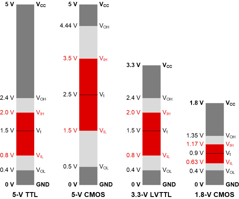 Figure 4-1 Logic
Thresholds
 -
Integrated Pulldown on Logic Pins : The logic inputs of TI muxes are CMOS inputs. Leaving the logic inputs of TI muxes floating is never recommended (See Implications of Slow or Floating CMOS Inputs) except when using a device that has integrated pulldown resistors on the logic pins. These resistors will hold the logic pin to a known state when not being driven high or low. This removes the need for additional external components, saving money and space.
- ON Resistance (RON): The resistance inserted into the signal
path as a result of the switch path being turned on. Because it contributes to
signal loss and degradation, low RON tradeoffs must be considered.
Noncharge-pump switches achieve low RON with large pass transistors.
These larger transistors lead to larger die sizes and increased Cio.
This additional channel capacitance can be very significant as it limits the
frequency response of the switch. As stated in Section 2.3, switches utilizing charge-pump technology can achieve low RON and
Cio, but require significantly higher ICC.
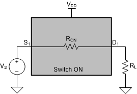 Figure 4-2 On-Resistance
 - Switch Output Level: The maximum signal level a switch without a charge pump can pass is typically limited to the switch VCC. Is there sufficient noise margin on the device downstream of the switch such that signal attenuation in the switch will not cause data errors? For instance, the N-channel transistor of a CBT device clamps the switch output at a little more than 1 V below the operating VCC, making it unsuitable for 5-V CMOS high-level (VIH = 3.5 V) signal transmission unless operated from at least 4.5-V VCC. This clamping won't be seen in devices with transmission gate architecture.
- ON/OFF Capacitance (CON/COFF): The
ON capacitive loading when a switch path is in the low impedance state. The OFF
capacitive loading when a switch path is in the high impedance state. Total
switch and load capacitance must be considered because it can affect response
time, settling time and fanout limits. See more details in the application note:
Improve Stability Issues with Low CON
Multiplexers. Cio is the capacitance of an
input/output (I/O) terminal of the device with the input conditions applied
that, according to the product specification, establishes the high-impedance
state at the output. This parameter is the internal capacitance encountered at
an input/output (I/O) of the device. These values are established by the design,
process, and package of the device.
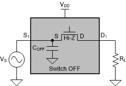 Figure 4-3 Source and Drain Off
CapacitanceFigure 4-4 Source and Drain On Capacitance
 - Frequency Response: All
CMOS switches have an upper limit to the frequency that can be passed. No matter
how low RON and Cio can be maintained in the chip
manufacturing process, they still form an undesired low-pass filter that
attenuates the switch output signal. Bandwidth (BW) of a switch is the
frequency range of signals that can pass through the switch with no more than 3
dB of attenuation.
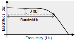 Figure 4-5 Bandwidth
 -
Latchup-Immunity : This feature prevents the device’s power rails from shorting together (latching up) due to electrical overstress, injected currents, or electrically fast transients. See Using Latch-Up Immune Multiplexers to Help Improve System Reliability for information on TI multiplexers Latch-Up Immunity.
- Sine-Wave Distortion or Total Harmonic Distortion: These are measurements of the linearity of the device. Nonlinearity can be introduced a number of ways (design, device physics, and so forth) but, typically, the largest contributor is RON. As shown in Figure 2-2 and Figure 2-4, RON varies with VI/O for all types of CMOS switches. Having a low RON is important, but a flat RON over the signal range is almost equally important.
- Crosstalk: There are two
types of crosstalk to consider:
- Channel-to-channel
crosstalk (XTALK): A measurement of unwanted signal
coupling from an ON channel to an OFF channel. This is measured in a
specific frequency and in specified in dB. The level of crosstalk is a
measure of how well decoupled the switch control signal is from the
switch output. Due to the parasitic capacitance of CMOS processes,
changing the state on the control signal causes noise to appear on the
output. In audio applications, this can be a source of the annoying pop
that is sometimes heard when switching the unit on or off. Devices such
as the TS5A22364 have built in shunt resistors that will discharge any
built up capacitance on the unselected signal path to reduce this
popping sound.
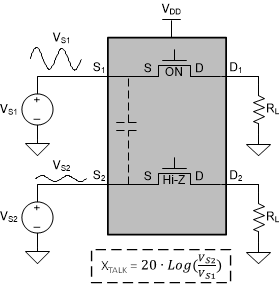 Figure 4-6 Channel-to-Channel Crosstalk
 - Crosstalk between switches. The level of crosstalk also is a measure of adjacent-channel rejection. As with control-to-output crosstalk, parasitic capacitance can couple the signal on one switch with that on another switch.
- Channel-to-channel
crosstalk (XTALK): A measurement of unwanted signal
coupling from an ON channel to an OFF channel. This is measured in a
specific frequency and in specified in dB. The level of crosstalk is a
measure of how well decoupled the switch control signal is from the
switch output. Due to the parasitic capacitance of CMOS processes,
changing the state on the control signal causes noise to appear on the
output. In audio applications, this can be a source of the annoying pop
that is sometimes heard when switching the unit on or off. Devices such
as the TS5A22364 have built in shunt resistors that will discharge any
built up capacitance on the unselected signal path to reduce this
popping sound.
- Charge Injection
(QC): Charge injection is a measurement of unwanted
signal coupling from the control (IN) input to the analog output. This is
measured in coulomb (C) and measured by the total charge induced due to
switching of the control input. TI specifies enable-to-output crosstalk and some
competitors use this parameter. As with enable-to-output crosstalk, changing the
state on the control pin causes a charge to be coupled to the channel of the
transistor introducing signal noise. It is presented in this report for a
relative comparison with the competition. TI muxes such as the TMUX1308,
TMUX1309 and SN74HC4851 have built in injection current control circuity to
shunt any injected current to ground, stabilizing the output signal. See more
details in Prevent crosstalk with injection current
control.
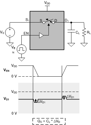 Figure 4-7 Charge
Injection
 - Off Isolation: A measurement OFF-state switch impedance.
This is measured in dB at a specific frequency, with the corresponding channel
in the OFF state.
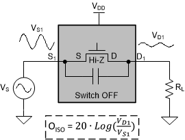 Figure 4-8 Off-Isolation
 - ON Leakage Current: Leakage current measured at the
input port in the ON state, with the corresponding output port in the ON state
and the output being open (See Figure 4-9). Leakage
current during the high-impedance state should be very small. Leakage current,
if high, may load an isolated bus and corrupt the data.
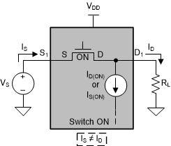 Figure 4-9 ON Leakage
Current
 - OFF Leakage Current: Leakage current measured at the
input port, with the corresponding channel output in the OFF state under
worst-case input and output conditions (See Figure 4-10) . Leakage
current is an important parameter, as it contributes to DC errors both when the
switch is ON and when it is OFF.
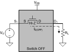 Figure 4-10 OFF Leakage
Current
 - Break-Before-Make Time (tBBM): Ensures that
in a multiplexer, two multiplexer paths are never electrically connected when
the signal path is changed by the select input. Break before make delay is a
safety feature that prevents two inputs from connecting when the device is
switching. The output first breaks from the ON-state switch before making the
connection with the next on-state switch. It guarantees that two multiplexer
paths are never electrically connected when the signal path is changed by the
select input. See Figure 4-11 for more
details.
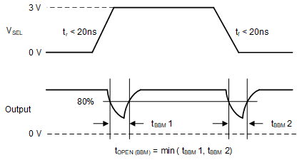 Figure 4-11 Break-Before-Make Time
(tBBM)
 - Turn ON (tON) /
Turn OFF (tOFF) Time: The time required for a switch path to
be internally changed to an ON or OFF state. These parameters determine how
quickly the switch can respond to a desired ON or OFF state (See Figure 4-12). In
general, switch enable and disable times are not symmetrical. This is not
usually an issue, as few applications require high control (enable) signal
frequencies. See more details on switch timing characteristics in Switches and muxes: What are timing
characteristics?.
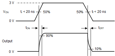 Figure 4-12 Turn-ON
(tON) and Turn-OFF (tOFF) Time
 - Propagation Delay (tpd): This is the time required for the signal to pass through the switch from the input to the output. This parameter is negligible for all but the most critical timing budgets. When the switch is ON, the propagation delay through one or more of the pass transistors is minimal. The load seen on the output of the switch and the driving strength at the input will typically have far greater contributions and limitations on the propagation delay and timing than the switch itself. The On-resistance and On-capacitance and load of the device can be used for a method to approximate the propagation delay.
- 1.8 V Control Logic: Switches with this feature have a built-in voltage translator to prevent voltage mismatch between the supply rail and the control logic. VIH and VIL levels are compatible with the 1.8-V logic levels at any voltage supply. See the Simplifying Design With 1.8 V logic MUXes and Switches Tech Note for more information. Most of the new TMUX devices (for example: TMUX1108, TMUX1511, TS3A27518E, TS5A26542) come with the 1.8 V control logic feature. The built-in voltage translator prevents voltage mismatch between the supply rail of the TMUX device and the control logic of the processor. This feature enables the mux to be controlled directly by the processor through standard 1.8 V GPIO pins. This eliminates the need for an external voltage translator, saving space in the system.
-
1.2V Control Logic : Similar to the 1.8V control logic, this feature allows for muxes, such as the TMUX1575, to be logic compatible with 1.2V logic levels reducing the need for an external voltage translator, saving space in the system.
-
Support Negative Voltage : This is defined as a multiplexer that allows negative voltages to be pass without the need for a dual supply. The TMUX4157N is an example of this with a single negative voltage supply, while TS5A22362 and TS5A22364 are both examples of devices that support negative analog signal pass through with only a positive single sided supply.
- Fail-safe Logic: Ensures the switch stays off and the
logic pin does not back-power VDD when the voltage on the signal pin is greater
than VDD. TI switches, such as TMUX1574, TMUX1575, TMUX72xx, TMUX73xx and
TMUX4157N, with Fail-safe Logic will protect downstream components when a logic
signal is present on the select pins while the switch is unpowered. This feature
allows voltages on the control pins to be applied before the supply pin,
protecting the device from potential damage. The switch maintains in a
high-impedance state on the SEL logic pins preventing power from going through
VDD during power sequencing. For example, the Fail-Safe Logic feature allows the
select pins of the TMUX1574 to be ramped to 5.5 V while supply VDD =
0 V. Additionally, the feature enables operation of the multiplexer with
VDD below the voltage on the select pins.
- Protects mux and downstream ICs from damage.
- Eliminates need for power sequencing solutions.
- Reduces BOM count and cost Simplifies system design.
- Improves system reliability.
See more details in What is fail-safe logic?.
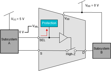 Figure 4-13 Fail-Safe
Logic