SLLA471B June 2021 – December 2021 CD4016B , CD4016B-MIL , CD4051B , CD4051B-MIL , CD4051B-Q1 , CD4052B , CD4052B-MIL , CD4053B , CD4053B-MIL , CD4053B-Q1 , CD4066B , CD4066B-MIL , CD4066B-Q1 , CD4067B , CD4067B-MIL , CD4097B , CD4097B-MIL , CD54HC4051 , CD54HC4052 , CD54HC4053 , CD54HC4066 , CD54HC4316 , CD54HC4351 , CD54HCT4051 , CD74HC4016 , CD74HC4051 , CD74HC4051-EP , CD74HC4051-Q1 , CD74HC4052 , CD74HC4053 , CD74HC4066 , CD74HC4067 , CD74HC4316 , CD74HC4351 , CD74HC4352 , CD74HCT4051 , CD74HCT4051-Q1 , CD74HCT4052 , CD74HCT4053 , CD74HCT4066 , CD74HCT4066-Q1 , CD74HCT4067 , CD74HCT4067-Q1 , CD74HCT4316 , CD74HCT4351 , LMH6580 , LMH6583 , LMH6586 , LMS4684 , MAX4594 , MAX4595 , MAX4596 , MAX4597 , MPC506 , MPC507 , MPC508 , MPC509 , MUX36D04 , MUX36D08 , MUX36S08 , MUX36S16 , MUX506 , MUX507 , MUX508 , MUX509 , SN3257-Q1 , SN54CBTD3384 , SN74AHC4066 , SN74AUC1G66 , SN74AUC2G53 , SN74AUC2G66 , SN74CB3Q16210 , SN74CB3Q16211 , SN74CB3Q16244 , SN74CB3Q16245 , SN74CB3Q16811 , SN74CB3Q3125 , SN74CB3Q3244 , SN74CB3Q3245 , SN74CB3Q3251 , SN74CB3Q3253 , SN74CB3Q3257 , SN74CB3Q3305 , SN74CB3Q3306A , SN74CB3Q3306A-EP , SN74CB3Q3345 , SN74CB3Q3384A , SN74CB3Q6800 , SN74CB3T16210 , SN74CB3T16210-Q1 , SN74CB3T16211 , SN74CB3T16212 , SN74CB3T1G125 , SN74CB3T1G125-Q1 , SN74CB3T3125 , SN74CB3T3245 , SN74CB3T3253 , SN74CB3T3257 , SN74CB3T3306 , SN74CB3T3383 , SN74CB3T3384 , SN74CBT16209A , SN74CBT16210 , SN74CBT16210C , SN74CBT16211A , SN74CBT16211C , SN74CBT16212A , SN74CBT16212C , SN74CBT16213 , SN74CBT16214 , SN74CBT16214C , SN74CBT162292 , SN74CBT16232 , SN74CBT16233 , SN74CBT16244 , SN74CBT16244C , SN74CBT16245 , SN74CBT16245C , SN74CBT16292 , SN74CBT16390 , SN74CBT16800C , SN74CBT16811C , SN74CBT16861 , SN74CBT1G125 , SN74CBT1G384 , SN74CBT3125 , SN74CBT3125C , SN74CBT3126 , SN74CBT3244 , SN74CBT3244C , SN74CBT3245A , SN74CBT3245C , SN74CBT3251 , SN74CBT3253 , SN74CBT3253C , SN74CBT3257 , SN74CBT3257C , SN74CBT3305C , SN74CBT3306 , SN74CBT3306C , SN74CBT3345 , SN74CBT3345C , SN74CBT3383 , SN74CBT3383C , SN74CBT3384A , SN74CBT3384C , SN74CBT34X245 , SN74CBT3861 , SN74CBT6800A , SN74CBT6800C , SN74CBT6845C , SN74CBTD16210 , SN74CBTD16211 , SN74CBTD1G125 , SN74CBTD1G384 , SN74CBTD3305C , SN74CBTD3306 , SN74CBTD3306C , SN74CBTD3384 , SN74CBTD3384C , SN74CBTD3861 , SN74CBTH16211 , SN74CBTK6800 , SN74CBTLV16210 , SN74CBTLV16211 , SN74CBTLV16212 , SN74CBTLV16292 , SN74CBTLV16800 , SN74CBTLV1G125 , SN74CBTLV1G125-Q1 , SN74CBTLV3125 , SN74CBTLV3126 , SN74CBTLV3245A , SN74CBTLV3251 , SN74CBTLV3253 , SN74CBTLV3257 , SN74CBTLV3257-EP , SN74CBTLV3383 , SN74CBTLV3384 , SN74CBTLV3857 , SN74CBTLV3861 , SN74CBTLV3861-Q1 , SN74CBTS16211 , SN74CBTS16212 , SN74CBTS3306 , SN74CBTS3384 , SN74CBTS6800 , SN74HC151-Q1 , SN74HC4066 , SN74HC4851 , SN74HC4851-Q1 , SN74HC4852 , SN74HC4852-Q1 , SN74LV4051A , SN74LV4051A-EP , SN74LV4051A-Q1 , SN74LV4052A , SN74LV4052A-EP , SN74LV4052A-Q1 , SN74LV4053A , SN74LV4053A-EP , SN74LV4053A-Q1 , SN74LV4066A , SN74LVC1G3157 , SN74LVC1G3157-Q1 , SN74LVC1G66 , SN74LVC1G66-Q1 , SN74LVC2G53 , SN74LVC2G66 , SN74LVC2G66-Q1 , SN74TVC16222A , SN74TVC3010 , SN74TVC3306 , TMUX1072 , TMUX1101 , TMUX1102 , TMUX1104 , TMUX1108 , TMUX1109 , TMUX1111 , TMUX1112 , TMUX1113 , TMUX1119 , TMUX1121 , TMUX1122 , TMUX1123 , TMUX1133 , TMUX1134 , TMUX1136 , TMUX1204 , TMUX1208 , TMUX1209 , TMUX1219 , TMUX1247 , TMUX1308 , TMUX1308-Q1 , TMUX1309 , TMUX136 , TMUX1511 , TMUX154E , TMUX1574 , TMUX6104 , TMUX6111 , TMUX6112 , TMUX6113 , TMUX6119 , TMUX6121 , TMUX6122 , TMUX6123 , TMUX6136 , TS12A12511 , TS12A44513 , TS12A44514 , TS12A44515 , TS12A4514 , TS12A4515 , TS12A4516 , TS12A4517 , TS3A24157 , TS3A24159 , TS3A27518E , TS3A27518E-Q1 , TS3A44159 , TS3A4741 , TS3A4742 , TS3A4751 , TS3A5017 , TS3A5017-Q1 , TS3A5018 , TS3A5223 , TS5A1066 , TS5A12301E , TS5A2053 , TS5A2066 , TS5A21366 , TS5A22362 , TS5A22364 , TS5A22364-Q1 , TS5A22366 , TS5A23157 , TS5A23157-Q1 , TS5A23159 , TS5A23160 , TS5A23166 , TS5A23167 , TS5A26542 , TS5A3153 , TS5A3154 , TS5A3157 , TS5A3159 , TS5A3159-EP , TS5A3159-Q1 , TS5A3159A , TS5A3160 , TS5A3166 , TS5A3166-Q1 , TS5A3167 , TS5A3357 , TS5A3357-Q1 , TS5A3359 , TS5A4594 , TS5A4595 , TS5A4596 , TS5A4597 , TS5A4624 , TS5A623157 , TS5A63157 , TS5A6542 , TS5A9411 , TS5MP645 , TS5MP646 , TS5N118 , TS5N214 , TS5N412
7 Timing Characteristics
For detailed information, see the Switches and muxes: What are timing characteristics? training video from TI Precision Labs.
For more parameter information, see the device data sheet.
| Transition time (tTRAN) — The time taken by the switch output to rise or fall within a given percentage of the final value after the address signal has risen or fallen past the logic threshold. |  Figure 7-1 Transition Time Figure 7-1 Transition Time |
| Device turn on time from enable pin (tON(EN) and tOFF(EN)) — The time taken by the switch output to rise or fall within a given percentage of the final value after the enable has risen or fallen past the logic threshold. |  Figure 7-2 Device Turn on Time From Enable Pin Figure 7-2 Device Turn on Time From Enable Pin |
| Break-before-make time (tOPEN (BBM)) — Ensures that in a multiplexer, two multiplexer paths are never electrically connected when the signal path is changed by the select input. |  Figure 7-3 Break-Before-Make Time Figure 7-3 Break-Before-Make Time |
| Make-before-break time (tCLOSED (MBB)) — Ensures that in a multiplexer, two multiplexer paths are never electrically disconnected when the signal path is changed by the select input. |  Figure 7-4 Make-Before-Break Time Figure 7-4 Make-Before-Break Time |
| Propagation delay through the switch (tpd) — The time required for a signal to pass from the input signal pin to the respective output signal pin. |  Figure 7-5 Propagation Delay Through the Switch Figure 7-5 Propagation Delay Through the Switch |
| Output-to-output skew (tSK) — The maximum difference between the propagation delays of different outputs due to different internal paths. | Figure 7-6 Output-to-Output Skew 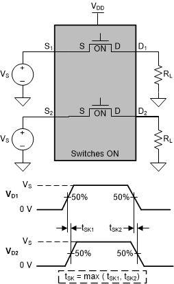 |
| Fault Response Time (tRESPONSE) - Fault response time (tRESPONSE) measures the delay between the source voltage exceeding the fault supply voltage (VFP or VFN) by 0.5V and the drain voltage failing to 90% of the fault supply voltage exceeded. This only applies to Fault Protected Devices. |  Figure 7-7 Fault
Response Time
Figure 7-7 Fault
Response Time |
| Fault Flag Response Time (tRESPONSE(FLAG)) - Fault flag response time (tRESPONSE(FLAG)) measures the delay between the source voltage exceeding the fault supply voltage (VFP or VFN) by 0.5 V and the general fault flag (FF) pin to go below 10% of its original value. This only applies to devices with an FF pin. |  Figure 7-8 Fault Flag
Response Time
Figure 7-8 Fault Flag
Response Time |
| Fault Drain Enable Time (tRESPONSE(DR)) -tRESPONSE(DR) represents the delay between the voltage at the DR pin falling from a high to low signal and the output of the drain pin reaching 90% of the fault supplies (VFP or VFN). tRESPONSE(DR) is a measure of how quickly the internal pull-up engages in response to the DR pin. Only on devices with a DR pin. |  Figure 7-9 Fault
Drain Enable Time
Figure 7-9 Fault
Drain Enable Time |
| Fault Recovery Time (tRECOVERY
) - Fault recovery time (tRECOVERY) measures the delay between the source voltage falling from overvoltage condition to below fault supply voltage (VFP or VFN) plus 0.5 V and the drain voltage rising from 0V to 50% of the fault supply voltage exceeded (only on fault protected devices). |  Figure 7-10 Fault
Recovery Time
Figure 7-10 Fault
Recovery Time |
| Fault Flag Recovery Time (tRECOVERY(FLAG)) – Fault flag recovery time (tRECOVERY(FLAG)) measures the delay between the source voltage falling from the overvoltage condition to below the fault supply voltage (VFP or VFN) plus 0.5 V and the general fault flag (FF) pin to rise above 3 V with 5 V external pull-up (only on devices with fault flags). |  Figure 7-11 Fault Flag
Recovery Time
Figure 7-11 Fault Flag
Recovery Time |